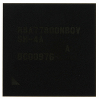
R8A77800ANBGAV Renesas Electronics America, R8A77800ANBGAV Datasheet - Page 1076

R8A77800ANBGAV
Manufacturer Part Number
R8A77800ANBGAV
Description
IC SUPERH MPU ROMLESS 449-BGA
Manufacturer
Renesas Electronics America
Series
SuperH® SH7780r
Datasheet
1.R8A77800ANBGV.pdf
(1342 pages)
Specifications of R8A77800ANBGAV
Core Processor
SH-4A
Core Size
32-Bit
Speed
400MHz
Connectivity
Audio Codec, MMC, Serial Sound, SCI, SIO, SPI, SSI
Peripherals
DMA, POR, WDT
Number Of I /o
75
Program Memory Type
ROMless
Ram Size
16K x 8
Voltage - Supply (vcc/vdd)
1.15 V ~ 1.35 V
Oscillator Type
External
Operating Temperature
-20°C ~ 75°C
Package / Case
449-BGA
Lead Free Status / RoHS Status
Lead free / RoHS Compliant
Eeprom Size
-
Program Memory Size
-
Data Converters
-
Available stocks
Company
Part Number
Manufacturer
Quantity
Price
Company:
Part Number:
R8A77800ANBGAV
Manufacturer:
Renesas Electronics America
Quantity:
10 000
- Current page: 1076 of 1342
- Download datasheet (7Mb)
Section 27 NAND Flash Memory Controller (FLCTL)
27.2
The pin configuration of the FLCTL is listed in table 27.1.
Table 27.1 Pin Configuration
Notes: 1. These pins are multiplexed with the H-UDI pins.
Rev.1.00 Dec. 13, 2005 Page 1024 of 1286
REJ09B0158-0100
Pin Name Function
FCE*
FD7 to
FD0*
FCLE*
FALE*
FRE*
FWE*
FRB *
—
FSE*
2
4
1
4
5
4
1
3
2. These pins are multiplexed with the INTC, H-UDI, GPIO, and mode control pins.
3. This pin is multiplexed with the SCIF channel 0, PCIC, and GPIO pin.
4. These pins are multiplexed with the SCIF0, HSPI, and GPIO pins.
5. This pin is multiplexed with the SCIF channel 0, HSPI, GPIO, and mode control pin.
Input/Output Pins
Chip enable
Data I/O pins
Command latch
enable
Output enable
Read Enable
Write enable
Ready/busy
—
Spare area
enable
I/O
Output
I/O
Output
Output
Output
Output
Input
—
Output
Corresponding
Flash Memory
Pin
NAND Type
CE
I/O7 to I/O0
CLE
ALE
RE
WE
R/B
WP
SE
Description
Enables flash memory connected to this
LSI.
I/O pins for command, address, and data.
Command Latch Enable (CLE)
Asserted when a command is output.
Address Latch Enable (ALE)
Asserted when an address is output and
negated when data is input or output.
Read Enable (RE)
Reads data at the falling edge of RE.
Write Enable
Flash memory latches a command,
address, and data at the rising edge of
WE.
Ready/Busy
Indicates ready state at high level;
indicates busy state at low level.
Write Protect/Reset (Not supported)
When this pin goes low, erroneous
erasure or programming at power on or
off can be prevented.
Spare Area Enable
Used to access spare area. This pin must
be fixed at low in sector access mode.
Related parts for R8A77800ANBGAV
Image
Part Number
Description
Manufacturer
Datasheet
Request
R

Part Number:
Description:
KIT STARTER FOR M16C/29
Manufacturer:
Renesas Electronics America
Datasheet:

Part Number:
Description:
KIT STARTER FOR R8C/2D
Manufacturer:
Renesas Electronics America
Datasheet:

Part Number:
Description:
R0K33062P STARTER KIT
Manufacturer:
Renesas Electronics America
Datasheet:

Part Number:
Description:
KIT STARTER FOR R8C/23 E8A
Manufacturer:
Renesas Electronics America
Datasheet:

Part Number:
Description:
KIT STARTER FOR R8C/25
Manufacturer:
Renesas Electronics America
Datasheet:

Part Number:
Description:
KIT STARTER H8S2456 SHARPE DSPLY
Manufacturer:
Renesas Electronics America
Datasheet:

Part Number:
Description:
KIT STARTER FOR R8C38C
Manufacturer:
Renesas Electronics America
Datasheet:

Part Number:
Description:
KIT STARTER FOR R8C35C
Manufacturer:
Renesas Electronics America
Datasheet:

Part Number:
Description:
KIT STARTER FOR R8CL3AC+LCD APPS
Manufacturer:
Renesas Electronics America
Datasheet:

Part Number:
Description:
KIT STARTER FOR RX610
Manufacturer:
Renesas Electronics America
Datasheet:

Part Number:
Description:
KIT STARTER FOR R32C/118
Manufacturer:
Renesas Electronics America
Datasheet:

Part Number:
Description:
KIT DEV RSK-R8C/26-29
Manufacturer:
Renesas Electronics America
Datasheet:

Part Number:
Description:
KIT STARTER FOR SH7124
Manufacturer:
Renesas Electronics America
Datasheet:

Part Number:
Description:
KIT STARTER FOR H8SX/1622
Manufacturer:
Renesas Electronics America
Datasheet:

Part Number:
Description:
KIT DEV FOR SH7203
Manufacturer:
Renesas Electronics America
Datasheet:


