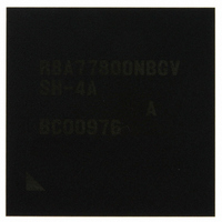
R8A77800ANBGAV Renesas Electronics America, R8A77800ANBGAV Datasheet - Page 425

R8A77800ANBGAV
Manufacturer Part Number
R8A77800ANBGAV
Description
IC SUPERH MPU ROMLESS 449-BGA
Manufacturer
Renesas Electronics America
Series
SuperH® SH7780r
Datasheet
1.R8A77800ANBGV.pdf
(1342 pages)
Specifications of R8A77800ANBGAV
Core Processor
SH-4A
Core Size
32-Bit
Speed
400MHz
Connectivity
Audio Codec, MMC, Serial Sound, SCI, SIO, SPI, SSI
Peripherals
DMA, POR, WDT
Number Of I /o
75
Program Memory Type
ROMless
Ram Size
16K x 8
Voltage - Supply (vcc/vdd)
1.15 V ~ 1.35 V
Oscillator Type
External
Operating Temperature
-20°C ~ 75°C
Package / Case
449-BGA
Lead Free Status / RoHS Status
Lead free / RoHS Compliant
Eeprom Size
-
Program Memory Size
-
Data Converters
-
Available stocks
Company
Part Number
Manufacturer
Quantity
Price
Company:
Part Number:
R8A77800ANBGAV
Manufacturer:
Renesas Electronics America
Quantity:
10 000
- Current page: 425 of 1342
- Download datasheet (7Mb)
Section 11 Local Bus State Controller (LBSC)
Bits PCWA/B1 and PCWA/B0 can be used to set the number of wait cycles to be inserted in a
low-speed bus cycle as 0, 15, 30, or 50. This value is added to the number of inserted wait cycles
specified by IW bit in CSnWCR or PCIW bit in CSnPCR. Bit TEDA/B (with a setting range from
0 to 15) can be used to ensure the setup times of the address, CE1A (CS5), CE1B (CS6), CE2A,
CE2B and REG to the RD and WE1 signals. Bits TEHA/B (with a setting range from 0 to15) can
be used to ensure the hold times of the address, CE1A (CS5), CE1B (CS6), CE2A, CE2B, and
REG to the RD and WE1 signals.
Bits IWW, IWRWD, IWRWS, IWRRD, and IWRRS in the CS5 bus control register (CS5BCR) or
CS6 bus control register (CS6BCR) are used to set the number of idle cycles between cycles. The
selected number of wait cycles between cycles depends only on the area to be accessed (area 5 or
6). When area 5 is accessed, bits IWW, IWRWD, IWRWS, IWRRD, and IWRRS in CS5BCR are
selected, and when area 6 is accessed, bits IWW, IWRWD, IWRWS, IWRRD, and IWRRS in
CS6BCR are selected.
In 32-byte transfer, a total of 32 bytes are transferred continuously according to the set bus width.
The first access is performed on the data for which there was an access request, and the remaining
accesses are performed in wraparound method according to the set bus width. The bus is not
released during this transfer.
ATA complement mode is to access the ATA device register connected to this LSI. The Device
Control Register, Alternate Status Register, Data Register, and Data Port can be accessed in ATA
complement mode.
To access the Device Control Register and Alternate Status Register, use a CPU byte access (do
not use a DMA transfer), and to access the Data Register, use the CPU word access (do not use a
DMA transfer). When a CPU byte access is executed, CE1x is negated and CE2x is asserted (x =
A, B). When a CPU word access is executed, CE1x is asserted and CE2x is negated.
To access the Data Port use a DMA transfer. The setting example of the DMAC is external
request, burst mode, level detection, overrun 0, DACK output to the correspondent PCMCIA
connected area. When DMA transfer of an ATA complement mode area is executed, neither
CE1x nor CE2x is asserted. Set the DACKBST bit in BCR of the corresponding DMA transfer
channel to 1, so that the corresponding DACK signal is asserted from the beginning to the end of
the DMA transfer cycle.
Specify the number of wait cycles between accesses as 0 for the DACK assertion area when
setting the DMA transfer size to 16-byte. After the DMA burst transfer that DACKBST was
enabled has finished, set the DACKBST bit to 1 again before starting the next DMA burst transfer.
Rev.1.00 Dec. 13, 2005 Page 373 of 1286
REJ09B0158-0100
Related parts for R8A77800ANBGAV
Image
Part Number
Description
Manufacturer
Datasheet
Request
R

Part Number:
Description:
KIT STARTER FOR M16C/29
Manufacturer:
Renesas Electronics America
Datasheet:

Part Number:
Description:
KIT STARTER FOR R8C/2D
Manufacturer:
Renesas Electronics America
Datasheet:

Part Number:
Description:
R0K33062P STARTER KIT
Manufacturer:
Renesas Electronics America
Datasheet:

Part Number:
Description:
KIT STARTER FOR R8C/23 E8A
Manufacturer:
Renesas Electronics America
Datasheet:

Part Number:
Description:
KIT STARTER FOR R8C/25
Manufacturer:
Renesas Electronics America
Datasheet:

Part Number:
Description:
KIT STARTER H8S2456 SHARPE DSPLY
Manufacturer:
Renesas Electronics America
Datasheet:

Part Number:
Description:
KIT STARTER FOR R8C38C
Manufacturer:
Renesas Electronics America
Datasheet:

Part Number:
Description:
KIT STARTER FOR R8C35C
Manufacturer:
Renesas Electronics America
Datasheet:

Part Number:
Description:
KIT STARTER FOR R8CL3AC+LCD APPS
Manufacturer:
Renesas Electronics America
Datasheet:

Part Number:
Description:
KIT STARTER FOR RX610
Manufacturer:
Renesas Electronics America
Datasheet:

Part Number:
Description:
KIT STARTER FOR R32C/118
Manufacturer:
Renesas Electronics America
Datasheet:

Part Number:
Description:
KIT DEV RSK-R8C/26-29
Manufacturer:
Renesas Electronics America
Datasheet:

Part Number:
Description:
KIT STARTER FOR SH7124
Manufacturer:
Renesas Electronics America
Datasheet:

Part Number:
Description:
KIT STARTER FOR H8SX/1622
Manufacturer:
Renesas Electronics America
Datasheet:

Part Number:
Description:
KIT DEV FOR SH7203
Manufacturer:
Renesas Electronics America
Datasheet:


