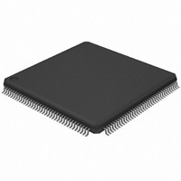
AT32UC3A364-ALUT Atmel, AT32UC3A364-ALUT Datasheet - Page 942

AT32UC3A364-ALUT
Manufacturer Part Number
AT32UC3A364-ALUT
Description
IC MCU 64KB FLASH 144LQFP
Manufacturer
Atmel
Series
AVR®32 UC3r
Specifications of AT32UC3A364-ALUT
Core Processor
AVR
Core Size
32-Bit
Speed
66MHz
Connectivity
EBI/EMI, I²C, IrDA, MMC, SPI, SSC, UART/USART, USB OTG
Peripherals
Brown-out Detect/Reset, DMA, POR, WDT
Number Of I /o
110
Program Memory Size
64KB (64K x 8)
Program Memory Type
FLASH
Ram Size
128K x 8
Voltage - Supply (vcc/vdd)
1.65 V ~ 1.95 V
Data Converters
A/D 8x10b
Oscillator Type
Internal
Operating Temperature
-40°C ~ 85°C
Package / Case
144-LQFP
Processor Series
AT32UC3x
Core
AVR32
Data Bus Width
32 bit
Data Ram Size
96 KB
Interface Type
IrDA/SCI/SCIF/UDI
Maximum Clock Frequency
66 MHz
Number Of Timers
3
Operating Supply Voltage
3 V to 3.6 V
Maximum Operating Temperature
+ 85 C
Mounting Style
SMD/SMT
3rd Party Development Tools
EWAVR32, EWAVR32-BL, KSK-EVK1100-PL
Development Tools By Supplier
ATAVRDRAGON, ATSTK500, ATSTK600, ATAVRISP2, ATAVRONEKIT, ATEXTWIFI, ATEVK1104
Minimum Operating Temperature
- 40 C
Controller Family/series
AT32UC3A
No. Of I/o's
110
Ram Memory Size
64KB
Cpu Speed
66MHz
No. Of Timers
2
Rohs Compliant
Yes
For Use With
ATEVK1104 - KIT DEV/EVAL FOR AVR32 AT32UC3AATAVRONEKIT - KIT AVR/AVR32 DEBUGGER/PROGRMMRATEVK1100 - KIT DEV/EVAL FOR AVR32 AT32UC3A
Lead Free Status / RoHS Status
Lead free / RoHS Compliant
Eeprom Size
-
Lead Free Status / Rohs Status
Lead free / RoHS Compliant
Available stocks
Company
Part Number
Manufacturer
Quantity
Price
- Current page: 942 of 1014
- Download datasheet (16Mb)
34.4.7
34.4.8
34.4.8.1
Figure 34-6. Scanning in JTAG Instruction
34.4.8.2
32072C–AVR32–2010/03
TCK
TAP State
TMS
TDI
TDO
How to Initialize the Module
Typical Sequence
Scanning in JTAG Instruction
Scanning in/out Data
TLR
Independent of the initial state of the TAP Controller, the Test-Logic-Reset state can always be
entered by holding TMS high for 5 TCK clock periods. This sequence should always be applied
at the start of a JTAG session to bring the TAP Controller into a defined state before applying
JTAG commands. Applying a 0 on TMS for 1 TCK period brings the TAP Controller to the Run-
Test/Idle state, which is the starting point for JTAG operations.
Assuming Run-Test/Idle is the present state, a typical scenario for using the JTAG Interface
follows.
At the TMS input, apply the sequence 1, 1, 0, 0 at the rising edges of TCK to enter the Shift
Instruction Register (Shift-IR) state. While in this state, shift the 5 bits of the JTAG instructions
into the JTAG instruction register from the TDI input at the rising edge of TCK. During shifting,
the JTAG outputs status bits on TDO, refer to
input must be held low during input of the 4 LSBs in order to remain in the Shift-IR state. The
JTAG Instruction selects a particular Data Register as path between TDI and TDO and controls
the circuitry surrounding the selected Data Register.
Apply the TMS sequence 1, 1, 0 to re-enter the Run-Test/Idle state. The instruction is latched
onto the parallel output from the shift register path in the Update-IR state. The Exit-IR, Pause-IR,
and Exit2-IR states are only used for navigating the state machine.
At the TMS input, apply the sequence 1, 0, 0 at the rising edges of TCK to enter the Shift Data
Register (Shift-DR) state. While in this state, upload the selected Data Register (selected by the
present JTAG instruction in the JTAG Instruction Register) from the TDI input at the rising edge
of TCK. In order to remain in the Shift-DR state, the TMS input must be held low. While the Data
Register is shifted in from the TDI pin, the parallel inputs to the Data Register captured in the
Capture-DR state is shifted out on the TDO pin.
RTI SelDR SelIR CapIR ShIR
Instruction
Section 34.5
ImplDefined
for a description of these. The TMS
AT32UC3A3/A4
Ex1IR UpdIR RTI
942
Related parts for AT32UC3A364-ALUT
Image
Part Number
Description
Manufacturer
Datasheet
Request
R

Part Number:
Description:
KIT DEV/EVAL FOR AT32UC3A3
Manufacturer:
Atmel
Datasheet:

Part Number:
Description:
DEV KIT FOR AVR/AVR32
Manufacturer:
Atmel
Datasheet:

Part Number:
Description:
INTERVAL AND WIPE/WASH WIPER CONTROL IC WITH DELAY
Manufacturer:
ATMEL Corporation
Datasheet:

Part Number:
Description:
Low-Voltage Voice-Switched IC for Hands-Free Operation
Manufacturer:
ATMEL Corporation
Datasheet:

Part Number:
Description:
MONOLITHIC INTEGRATED FEATUREPHONE CIRCUIT
Manufacturer:
ATMEL Corporation
Datasheet:

Part Number:
Description:
AM-FM Receiver IC U4255BM-M
Manufacturer:
ATMEL Corporation
Datasheet:

Part Number:
Description:
Monolithic Integrated Feature Phone Circuit
Manufacturer:
ATMEL Corporation
Datasheet:

Part Number:
Description:
Multistandard Video-IF and Quasi Parallel Sound Processing
Manufacturer:
ATMEL Corporation
Datasheet:

Part Number:
Description:
High-performance EE PLD
Manufacturer:
ATMEL Corporation
Datasheet:

Part Number:
Description:
8-bit Flash Microcontroller
Manufacturer:
ATMEL Corporation
Datasheet:

Part Number:
Description:
2-Wire Serial EEPROM
Manufacturer:
ATMEL Corporation
Datasheet:


