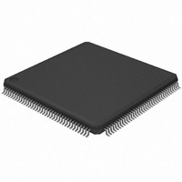
AT32UC3A364-ALUT Atmel, AT32UC3A364-ALUT Datasheet - Page 168

AT32UC3A364-ALUT
Manufacturer Part Number
AT32UC3A364-ALUT
Description
IC MCU 64KB FLASH 144LQFP
Manufacturer
Atmel
Series
AVR®32 UC3r
Specifications of AT32UC3A364-ALUT
Core Processor
AVR
Core Size
32-Bit
Speed
66MHz
Connectivity
EBI/EMI, I²C, IrDA, MMC, SPI, SSC, UART/USART, USB OTG
Peripherals
Brown-out Detect/Reset, DMA, POR, WDT
Number Of I /o
110
Program Memory Size
64KB (64K x 8)
Program Memory Type
FLASH
Ram Size
128K x 8
Voltage - Supply (vcc/vdd)
1.65 V ~ 1.95 V
Data Converters
A/D 8x10b
Oscillator Type
Internal
Operating Temperature
-40°C ~ 85°C
Package / Case
144-LQFP
Processor Series
AT32UC3x
Core
AVR32
Data Bus Width
32 bit
Data Ram Size
96 KB
Interface Type
IrDA/SCI/SCIF/UDI
Maximum Clock Frequency
66 MHz
Number Of Timers
3
Operating Supply Voltage
3 V to 3.6 V
Maximum Operating Temperature
+ 85 C
Mounting Style
SMD/SMT
3rd Party Development Tools
EWAVR32, EWAVR32-BL, KSK-EVK1100-PL
Development Tools By Supplier
ATAVRDRAGON, ATSTK500, ATSTK600, ATAVRISP2, ATAVRONEKIT, ATEXTWIFI, ATEVK1104
Minimum Operating Temperature
- 40 C
Controller Family/series
AT32UC3A
No. Of I/o's
110
Ram Memory Size
64KB
Cpu Speed
66MHz
No. Of Timers
2
Rohs Compliant
Yes
For Use With
ATEVK1104 - KIT DEV/EVAL FOR AVR32 AT32UC3AATAVRONEKIT - KIT AVR/AVR32 DEBUGGER/PROGRMMRATEVK1100 - KIT DEV/EVAL FOR AVR32 AT32UC3A
Lead Free Status / RoHS Status
Lead free / RoHS Compliant
Eeprom Size
-
Lead Free Status / Rohs Status
Lead free / RoHS Compliant
Available stocks
Company
Part Number
Manufacturer
Quantity
Price
- Current page: 168 of 1014
- Download datasheet (16Mb)
14.6.5.2
32072C–AVR32–2010/03
CFCE1 and CFCE2 signals
To cover all types of access, the SMC must be alternatively set to drive 8-bit data bus or 16-bit
data bus. The odd byte access on the DATA[7:0] bus is only possible when the SMC is config-
ured to drive 8-bit memory devices on the corresponding NCS pin (NCS[4] or NCS[5]). The Data
Bus Width (DBW) field in the SMC Mode (MODE) register of the NCS[4] and/or NCS[5] address
space must be written as shown in
NBS1 and NBS0 are the byte selection signals from SMC and are available when the SMC is set
in Byte Select mode on the corresponding Chip Select.
The CFCE1 and CFCE2 waveforms are identical to the corresponding NCSx waveform. For
details on these waveforms and timings, refer to the SMC Section.
Table 14-5.
Common Memory
Address Space is
Attribute Memory
Standby Mode or
Control Register
Alternate Status
not assigned to
Drive Address
Data Register
I/O Mode
Task File
Mode
Read
CF
CFCE1 and CFCE2 Truth Table
CFCE2
NBS1
NBS1
NBS1
1
1
1
1
0
0
1
CFCE1
NBS0
NBS0
NBS0
0
0
0
0
1
1
1
Table 14-5 on page 168
Alternate True IDE Mode
16 bits
16 bits
16 bits
16bits
DBW
8 bits
8 bits
8 bits
8 bits
Don’t
Care
True IDE Mode
–
Comment
Access to Even Byte on
DATA[7:0]
Access to Even Byte on
DATA[7:0]
Access to Odd Byte on
DATA[15:8]
Access to Odd Byte on
DATA[7:0]
Access to Even Byte on
DATA[7:0]
Access to Odd Byte on
DATA[15:8]
Access to Odd Byte on
DATA[7:0]
Access to Even Byte on
DATA[7:0]
Access to Odd Byte on
DATA[7:0]
Access to Even Byte on
DATA[7:0]
Access to Odd Byte on
DATA[15:8]
Access to Even Byte on
DATA[7:0]
Access to Odd Byte on
DATA[7:0]
to enable the required access type.
–
AT32UC3A3/A4
SMC Access
Mode
Byte Select
Byte Select
Byte Select
Byte Select
Don’t Care
–
168
Related parts for AT32UC3A364-ALUT
Image
Part Number
Description
Manufacturer
Datasheet
Request
R

Part Number:
Description:
KIT DEV/EVAL FOR AT32UC3A3
Manufacturer:
Atmel
Datasheet:

Part Number:
Description:
DEV KIT FOR AVR/AVR32
Manufacturer:
Atmel
Datasheet:

Part Number:
Description:
INTERVAL AND WIPE/WASH WIPER CONTROL IC WITH DELAY
Manufacturer:
ATMEL Corporation
Datasheet:

Part Number:
Description:
Low-Voltage Voice-Switched IC for Hands-Free Operation
Manufacturer:
ATMEL Corporation
Datasheet:

Part Number:
Description:
MONOLITHIC INTEGRATED FEATUREPHONE CIRCUIT
Manufacturer:
ATMEL Corporation
Datasheet:

Part Number:
Description:
AM-FM Receiver IC U4255BM-M
Manufacturer:
ATMEL Corporation
Datasheet:

Part Number:
Description:
Monolithic Integrated Feature Phone Circuit
Manufacturer:
ATMEL Corporation
Datasheet:

Part Number:
Description:
Multistandard Video-IF and Quasi Parallel Sound Processing
Manufacturer:
ATMEL Corporation
Datasheet:

Part Number:
Description:
High-performance EE PLD
Manufacturer:
ATMEL Corporation
Datasheet:

Part Number:
Description:
8-bit Flash Microcontroller
Manufacturer:
ATMEL Corporation
Datasheet:

Part Number:
Description:
2-Wire Serial EEPROM
Manufacturer:
ATMEL Corporation
Datasheet:


