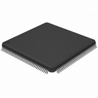
AT32UC3A364-ALUT Atmel, AT32UC3A364-ALUT Datasheet - Page 336

AT32UC3A364-ALUT
Manufacturer Part Number
AT32UC3A364-ALUT
Description
IC MCU 64KB FLASH 144LQFP
Manufacturer
Atmel
Series
AVR®32 UC3r
Specifications of AT32UC3A364-ALUT
Core Processor
AVR
Core Size
32-Bit
Speed
66MHz
Connectivity
EBI/EMI, I²C, IrDA, MMC, SPI, SSC, UART/USART, USB OTG
Peripherals
Brown-out Detect/Reset, DMA, POR, WDT
Number Of I /o
110
Program Memory Size
64KB (64K x 8)
Program Memory Type
FLASH
Ram Size
128K x 8
Voltage - Supply (vcc/vdd)
1.65 V ~ 1.95 V
Data Converters
A/D 8x10b
Oscillator Type
Internal
Operating Temperature
-40°C ~ 85°C
Package / Case
144-LQFP
Processor Series
AT32UC3x
Core
AVR32
Data Bus Width
32 bit
Data Ram Size
96 KB
Interface Type
IrDA/SCI/SCIF/UDI
Maximum Clock Frequency
66 MHz
Number Of Timers
3
Operating Supply Voltage
3 V to 3.6 V
Maximum Operating Temperature
+ 85 C
Mounting Style
SMD/SMT
3rd Party Development Tools
EWAVR32, EWAVR32-BL, KSK-EVK1100-PL
Development Tools By Supplier
ATAVRDRAGON, ATSTK500, ATSTK600, ATAVRISP2, ATAVRONEKIT, ATEXTWIFI, ATEVK1104
Minimum Operating Temperature
- 40 C
Controller Family/series
AT32UC3A
No. Of I/o's
110
Ram Memory Size
64KB
Cpu Speed
66MHz
No. Of Timers
2
Rohs Compliant
Yes
For Use With
ATEVK1104 - KIT DEV/EVAL FOR AVR32 AT32UC3AATAVRONEKIT - KIT AVR/AVR32 DEBUGGER/PROGRMMRATEVK1100 - KIT DEV/EVAL FOR AVR32 AT32UC3A
Lead Free Status / RoHS Status
Lead free / RoHS Compliant
Eeprom Size
-
Lead Free Status / Rohs Status
Lead free / RoHS Compliant
Available stocks
Company
Part Number
Manufacturer
Quantity
Price
- Current page: 336 of 1014
- Download datasheet (16Mb)
32072C–AVR32–2010/03
Figure 19-13. Multi-Block DMA Transfer with Source Address Auto-reloaded and Linked List
The DMA Transfer flow is shown in
17. The DMACA fetches the next LLI from memory location pointed to by the current LLPx
b. If interrupts are disabled (CTLx.INT_EN = 0) or the block complete interrupt is
register, and automatically reprograms the DARx, CTLx and LLPx channel registers.
Note that the SARx is not re-programmed as the reloaded value is used for the next
DMA block transfer. If the next block is the last block of the DMA transfer then the CTLx
and LLPx registers just fetched from the LLI should match Row 1 or Row 5 of
1 on page
336.
Address of
Source Layer
block complete interrupt when the block transfer has completed. It then stalls until
the block complete interrupt is cleared by software. If the next block is to be the last
block in the DMA transfer, then the block complete ISR (interrupt service routine)
should clear the CFGx.RELOAD_SR source reload bit. This puts the DMACA into
Row1 as shown in
the DMA transfer, then the source reload bit should remain enabled to keep the
DMACA in Row 7 as shown in
masked (MaskBlock[x] = 1’b0, where x is the channel number) then hardware does
not stall until it detects a write to the block complete interrupt clear register but
starts the next block transfer immediately. In this case, software must clear the
source reload bit, CFGx.RELOAD_SR, to put the device into Row 1 of
on page 324
Destination Address
SAR
324. The DMA transfer might look like that shown in
Source Blocks
before the last block of the DMA transfer has completed.
Table 19-1 on page
Figure 19-14 on page
Table 19-1 on page
324. If the next block is not the last block in
DAR(N)
DAR(1)
DAR(2)
DAR(0)
Destination Blocks
BlockN
Block0
Block1
Block2
337.
324.
AT32UC3A3/A4
Figure 19-13 on page
Destination Layer
Address of
Table 19-1
Table 19-
336
Related parts for AT32UC3A364-ALUT
Image
Part Number
Description
Manufacturer
Datasheet
Request
R

Part Number:
Description:
KIT DEV/EVAL FOR AT32UC3A3
Manufacturer:
Atmel
Datasheet:

Part Number:
Description:
DEV KIT FOR AVR/AVR32
Manufacturer:
Atmel
Datasheet:

Part Number:
Description:
INTERVAL AND WIPE/WASH WIPER CONTROL IC WITH DELAY
Manufacturer:
ATMEL Corporation
Datasheet:

Part Number:
Description:
Low-Voltage Voice-Switched IC for Hands-Free Operation
Manufacturer:
ATMEL Corporation
Datasheet:

Part Number:
Description:
MONOLITHIC INTEGRATED FEATUREPHONE CIRCUIT
Manufacturer:
ATMEL Corporation
Datasheet:

Part Number:
Description:
AM-FM Receiver IC U4255BM-M
Manufacturer:
ATMEL Corporation
Datasheet:

Part Number:
Description:
Monolithic Integrated Feature Phone Circuit
Manufacturer:
ATMEL Corporation
Datasheet:

Part Number:
Description:
Multistandard Video-IF and Quasi Parallel Sound Processing
Manufacturer:
ATMEL Corporation
Datasheet:

Part Number:
Description:
High-performance EE PLD
Manufacturer:
ATMEL Corporation
Datasheet:

Part Number:
Description:
8-bit Flash Microcontroller
Manufacturer:
ATMEL Corporation
Datasheet:

Part Number:
Description:
2-Wire Serial EEPROM
Manufacturer:
ATMEL Corporation
Datasheet:


