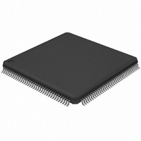
AT32UC3A364-ALUT Atmel, AT32UC3A364-ALUT Datasheet - Page 840

AT32UC3A364-ALUT
Manufacturer Part Number
AT32UC3A364-ALUT
Description
IC MCU 64KB FLASH 144LQFP
Manufacturer
Atmel
Series
AVR®32 UC3r
Specifications of AT32UC3A364-ALUT
Core Processor
AVR
Core Size
32-Bit
Speed
66MHz
Connectivity
EBI/EMI, I²C, IrDA, MMC, SPI, SSC, UART/USART, USB OTG
Peripherals
Brown-out Detect/Reset, DMA, POR, WDT
Number Of I /o
110
Program Memory Size
64KB (64K x 8)
Program Memory Type
FLASH
Ram Size
128K x 8
Voltage - Supply (vcc/vdd)
1.65 V ~ 1.95 V
Data Converters
A/D 8x10b
Oscillator Type
Internal
Operating Temperature
-40°C ~ 85°C
Package / Case
144-LQFP
Processor Series
AT32UC3x
Core
AVR32
Data Bus Width
32 bit
Data Ram Size
96 KB
Interface Type
IrDA/SCI/SCIF/UDI
Maximum Clock Frequency
66 MHz
Number Of Timers
3
Operating Supply Voltage
3 V to 3.6 V
Maximum Operating Temperature
+ 85 C
Mounting Style
SMD/SMT
3rd Party Development Tools
EWAVR32, EWAVR32-BL, KSK-EVK1100-PL
Development Tools By Supplier
ATAVRDRAGON, ATSTK500, ATSTK600, ATAVRISP2, ATAVRONEKIT, ATEXTWIFI, ATEVK1104
Minimum Operating Temperature
- 40 C
Controller Family/series
AT32UC3A
No. Of I/o's
110
Ram Memory Size
64KB
Cpu Speed
66MHz
No. Of Timers
2
Rohs Compliant
Yes
For Use With
ATEVK1104 - KIT DEV/EVAL FOR AVR32 AT32UC3AATAVRONEKIT - KIT AVR/AVR32 DEBUGGER/PROGRMMRATEVK1100 - KIT DEV/EVAL FOR AVR32 AT32UC3A
Lead Free Status / RoHS Status
Lead free / RoHS Compliant
Eeprom Size
-
Lead Free Status / Rohs Status
Lead free / RoHS Compliant
Available stocks
Company
Part Number
Manufacturer
Quantity
Price
- Current page: 840 of 1014
- Download datasheet (16Mb)
30.6.4.4
30.6.5
30.6.5.1
32072C–AVR32–2010/03
SD/SDIO Card Operation
READ_MULTIPLE_BLOCK
SDIO Data Transfer Type
The MCI allows processing of SD Memory (Secure Digital Memory Card) and SDIO (SD Input
Output) Card commands.
SD/SDIO cards are based on the MultiMedia Card (MMC) format, but are physically slightly
thicker and feature higher data transfer rates, a lock switch on the side to prevent accidental
overwriting and security features. The physical form factor, pin assignment and data transfer
protocol are forward-compatible with the MultiMedia Card with some additions. SD slots can
actually be used for more than flash memory cards. Devices that support SDIO can use small
devices designed for the SD form factor, such as GPS receivers, Wi-Fi or Bluetooth adapters,
modems, barcode readers, IrDA adapters, FM radio tuners, RFID readers, digital cameras and
more.
SD/SDIO is covered by numerous patents and trademarks, and licensing is only available
through the Secure Digital Card Association.
The SD/SDIO Card communication is based on a nine-pin interface (Clock, Command,
four Data and three Power lines). The communication protocol is defined as a part of this speci-
fication. The main difference between the SD/SDIO Card and the MultiMedia Card is the
initialization process.
The SD/SDIO Card Register (SDCR) allows selection of the Card Slot (SDCSEL) and the data
bus width (SDCBUS).
The SD/SDIO Card bus allows dynamic configuration of the number of data lines. After power
up, by default, the SD/SDIO Card uses only DAT[0] for data transfer. After initialization, the host
can change the bus width (number of active data lines).
SDIO cards may transfer data in either a multi-byte (1 to 512 bytes) or an optional block format
(1 to 511 blocks), while the SD memory cards are fixed in the block transfer mode. The
CMDR.TRTYP field allows to choose between SDIO Byte or SDIO Block transfer.
The number of bytes/blocks to transfer is set through the BCNT field in the BLKR register. In
SDIO Block mode, the field BLKLEN must be set to the data block size while this field is not
used in SDIO Byte mode.
1. Wait until the current command execution has successfully terminated.
2. Write the block length in the card. This value defines the value block_lenght.
3. Write the MR.BLKLEN with block_lenght value.
4. Program the DMA Controller to use a list of descriptors.
5. Write the DMA register with the following fields:
6. Write a one to the IER.DMADONE bit.
7. Issue a READ_MULTIPLE_BLOCK command.
8. Wait for DMA end of chained buffer transfer interrupt.
a. Check that the SR.CMDRDY and the SR.NOTBUSY are set.
– Write zero to the DMA.OFFSET.
– Write the DMA.CHKSIZE.
– Write a one to the DMA.DMAEN bit to enable DMA hardware handshaking in the
MCI.
AT32UC3A3/A4
840
Related parts for AT32UC3A364-ALUT
Image
Part Number
Description
Manufacturer
Datasheet
Request
R

Part Number:
Description:
KIT DEV/EVAL FOR AT32UC3A3
Manufacturer:
Atmel
Datasheet:

Part Number:
Description:
DEV KIT FOR AVR/AVR32
Manufacturer:
Atmel
Datasheet:

Part Number:
Description:
INTERVAL AND WIPE/WASH WIPER CONTROL IC WITH DELAY
Manufacturer:
ATMEL Corporation
Datasheet:

Part Number:
Description:
Low-Voltage Voice-Switched IC for Hands-Free Operation
Manufacturer:
ATMEL Corporation
Datasheet:

Part Number:
Description:
MONOLITHIC INTEGRATED FEATUREPHONE CIRCUIT
Manufacturer:
ATMEL Corporation
Datasheet:

Part Number:
Description:
AM-FM Receiver IC U4255BM-M
Manufacturer:
ATMEL Corporation
Datasheet:

Part Number:
Description:
Monolithic Integrated Feature Phone Circuit
Manufacturer:
ATMEL Corporation
Datasheet:

Part Number:
Description:
Multistandard Video-IF and Quasi Parallel Sound Processing
Manufacturer:
ATMEL Corporation
Datasheet:

Part Number:
Description:
High-performance EE PLD
Manufacturer:
ATMEL Corporation
Datasheet:

Part Number:
Description:
8-bit Flash Microcontroller
Manufacturer:
ATMEL Corporation
Datasheet:

Part Number:
Description:
2-Wire Serial EEPROM
Manufacturer:
ATMEL Corporation
Datasheet:


