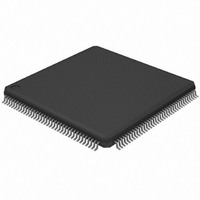
AT32UC3A364-ALUT Atmel, AT32UC3A364-ALUT Datasheet - Page 795

AT32UC3A364-ALUT
Manufacturer Part Number
AT32UC3A364-ALUT
Description
IC MCU 64KB FLASH 144LQFP
Manufacturer
Atmel
Series
AVR®32 UC3r
Specifications of AT32UC3A364-ALUT
Core Processor
AVR
Core Size
32-Bit
Speed
66MHz
Connectivity
EBI/EMI, I²C, IrDA, MMC, SPI, SSC, UART/USART, USB OTG
Peripherals
Brown-out Detect/Reset, DMA, POR, WDT
Number Of I /o
110
Program Memory Size
64KB (64K x 8)
Program Memory Type
FLASH
Ram Size
128K x 8
Voltage - Supply (vcc/vdd)
1.65 V ~ 1.95 V
Data Converters
A/D 8x10b
Oscillator Type
Internal
Operating Temperature
-40°C ~ 85°C
Package / Case
144-LQFP
Processor Series
AT32UC3x
Core
AVR32
Data Bus Width
32 bit
Data Ram Size
96 KB
Interface Type
IrDA/SCI/SCIF/UDI
Maximum Clock Frequency
66 MHz
Number Of Timers
3
Operating Supply Voltage
3 V to 3.6 V
Maximum Operating Temperature
+ 85 C
Mounting Style
SMD/SMT
3rd Party Development Tools
EWAVR32, EWAVR32-BL, KSK-EVK1100-PL
Development Tools By Supplier
ATAVRDRAGON, ATSTK500, ATSTK600, ATAVRISP2, ATAVRONEKIT, ATEXTWIFI, ATEVK1104
Minimum Operating Temperature
- 40 C
Controller Family/series
AT32UC3A
No. Of I/o's
110
Ram Memory Size
64KB
Cpu Speed
66MHz
No. Of Timers
2
Rohs Compliant
Yes
For Use With
ATEVK1104 - KIT DEV/EVAL FOR AVR32 AT32UC3AATAVRONEKIT - KIT AVR/AVR32 DEBUGGER/PROGRMMRATEVK1100 - KIT DEV/EVAL FOR AVR32 AT32UC3A
Lead Free Status / RoHS Status
Lead free / RoHS Compliant
Eeprom Size
-
Lead Free Status / Rohs Status
Lead free / RoHS Compliant
Available stocks
Company
Part Number
Manufacturer
Quantity
Price
- Current page: 795 of 1014
- Download datasheet (16Mb)
28.5.2
28.5.3
28.5.4
28.5.5
28.5.6
28.6
28.6.1
28.6.2
28.6.3
32072C–AVR32–2010/03
Functional Description
Power Management
Clocks
Interrupts
Analog Inputs
Timer Triggers
Analog-to-digital Conversion
Conversion Reference
Conversion Resolution
In sleep mode, the ADC clock is automatically stopped after each conversion. As the logic is
small and the ADC cell can be put into sleep mode, the Power Manager has no effect on the
ADC behavior.
The clock for the ADC bus interface (CLK_ADC) is generated by the Power Manager. This clock
is enabled at reset, and can be disabled in the Power Manager. It is recommended to disable the
ADC before disabling the clock, to avoid freezing the ADC in an undefined state.
The ADC interrupt request line is connected to the interrupt controller. Using the ADC interrupt
requires the interrupt controller to be programmed first.
The analog input pins can be multiplexed with I/O lines. In this case, the assignment of the ADC
input is automatically done as soon as the corresponding I/O is configured through the I/O con-
toller. By default, after reset, the I/O line is configured as a logic input.
Timer Counters may or may not be used as hardware triggers depending on user requirements.
Thus, some or all of the timer counters may be non-connected.
The ADC uses the ADC Clock to perform conversions. Converting a single analog value to a 10-
bit digital data requires sample and hold clock cycles as defined in the Sample and Hold Time
field of the Mode Register (MR.SHTIM) and 10 ADC Clock cycles. The ADC Clock frequency is
selected in the Prescaler Rate Selection field of the MR register (MR.PRESCAL).
The ADC Clock range is between CLK_ADC/2, if the PRESCAL field is 0, and CLK_ADC/128, if
the PRESCAL field is 63 (0x3F). The PRESCAL field must be written in order to provide an ADC
Clock frequency according to the parameters given in the Electrical Characteristics chapter.
The conversion is performed on a full range between 0V and the reference voltage connected to
VDDANA. Analog input values between these voltages are converted to digital values based on
a linear conversion.
The ADC supports 8-bit or 10-bit resolutions. The 8-bit selection is performed by writing a one to
the Resolution bit in the MR register (MR.LOWRES). By default, after a reset, the resolution is
the highest and the Converted Data field in the Channel Data Registers (CDRn.DATA) is fully
used. By writing a one to the LOWRES bit, the ADC switches in the lowest resolution and the
conversion results can be read in the eight lowest significant bits of the Channel Data Registers
(CDRn). The two highest bits of the DATA field in the corresponding CDRn register will be read
as zero. The two highest bits of the Last Data Converted field in the Last Converted Data Regis-
ter (LCDR.LDATA) will be read as zero too.
AT32UC3A3/A4
795
Related parts for AT32UC3A364-ALUT
Image
Part Number
Description
Manufacturer
Datasheet
Request
R

Part Number:
Description:
KIT DEV/EVAL FOR AT32UC3A3
Manufacturer:
Atmel
Datasheet:

Part Number:
Description:
DEV KIT FOR AVR/AVR32
Manufacturer:
Atmel
Datasheet:

Part Number:
Description:
INTERVAL AND WIPE/WASH WIPER CONTROL IC WITH DELAY
Manufacturer:
ATMEL Corporation
Datasheet:

Part Number:
Description:
Low-Voltage Voice-Switched IC for Hands-Free Operation
Manufacturer:
ATMEL Corporation
Datasheet:

Part Number:
Description:
MONOLITHIC INTEGRATED FEATUREPHONE CIRCUIT
Manufacturer:
ATMEL Corporation
Datasheet:

Part Number:
Description:
AM-FM Receiver IC U4255BM-M
Manufacturer:
ATMEL Corporation
Datasheet:

Part Number:
Description:
Monolithic Integrated Feature Phone Circuit
Manufacturer:
ATMEL Corporation
Datasheet:

Part Number:
Description:
Multistandard Video-IF and Quasi Parallel Sound Processing
Manufacturer:
ATMEL Corporation
Datasheet:

Part Number:
Description:
High-performance EE PLD
Manufacturer:
ATMEL Corporation
Datasheet:

Part Number:
Description:
8-bit Flash Microcontroller
Manufacturer:
ATMEL Corporation
Datasheet:

Part Number:
Description:
2-Wire Serial EEPROM
Manufacturer:
ATMEL Corporation
Datasheet:


