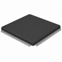
AT32UC3A364-ALUT Atmel, AT32UC3A364-ALUT Datasheet - Page 221

AT32UC3A364-ALUT
Manufacturer Part Number
AT32UC3A364-ALUT
Description
IC MCU 64KB FLASH 144LQFP
Manufacturer
Atmel
Series
AVR®32 UC3r
Specifications of AT32UC3A364-ALUT
Core Processor
AVR
Core Size
32-Bit
Speed
66MHz
Connectivity
EBI/EMI, I²C, IrDA, MMC, SPI, SSC, UART/USART, USB OTG
Peripherals
Brown-out Detect/Reset, DMA, POR, WDT
Number Of I /o
110
Program Memory Size
64KB (64K x 8)
Program Memory Type
FLASH
Ram Size
128K x 8
Voltage - Supply (vcc/vdd)
1.65 V ~ 1.95 V
Data Converters
A/D 8x10b
Oscillator Type
Internal
Operating Temperature
-40°C ~ 85°C
Package / Case
144-LQFP
Processor Series
AT32UC3x
Core
AVR32
Data Bus Width
32 bit
Data Ram Size
96 KB
Interface Type
IrDA/SCI/SCIF/UDI
Maximum Clock Frequency
66 MHz
Number Of Timers
3
Operating Supply Voltage
3 V to 3.6 V
Maximum Operating Temperature
+ 85 C
Mounting Style
SMD/SMT
3rd Party Development Tools
EWAVR32, EWAVR32-BL, KSK-EVK1100-PL
Development Tools By Supplier
ATAVRDRAGON, ATSTK500, ATSTK600, ATAVRISP2, ATAVRONEKIT, ATEXTWIFI, ATEVK1104
Minimum Operating Temperature
- 40 C
Controller Family/series
AT32UC3A
No. Of I/o's
110
Ram Memory Size
64KB
Cpu Speed
66MHz
No. Of Timers
2
Rohs Compliant
Yes
For Use With
ATEVK1104 - KIT DEV/EVAL FOR AVR32 AT32UC3AATAVRONEKIT - KIT AVR/AVR32 DEBUGGER/PROGRMMRATEVK1100 - KIT DEV/EVAL FOR AVR32 AT32UC3A
Lead Free Status / RoHS Status
Lead free / RoHS Compliant
Eeprom Size
-
Lead Free Status / Rohs Status
Lead free / RoHS Compliant
Available stocks
Company
Part Number
Manufacturer
Quantity
Price
- Current page: 221 of 1014
- Download datasheet (16Mb)
16.6.2
16.6.3
16.6.4
16.7
16.7.1
32072C–AVR32–2010/03
Functional Description
Power Management
Clocks
Interrupts
SDRAM Device Initialization
The SDRAMC must be properly stopped before entering in reset mode, i.e., the user must issue
a Deep power mode command in the Mode (MD) register and wait for the command to be
completed.
The clock for the SDRAMC bus interface (CLK_SDRAMC) is generated by the Power Manager.
This clock is enabled at reset, and can be disabled in the Power Manager. It is recommended to
disable the SDRAMC before disabling the clock, to avoid freezing the SDRAMC in an undefined
state.
The SDRAMC interrupt request line is connected to the interrupt controller. Using the SDRAMC
interrupt requires the interrupt controller to be programmed first.
The initialization sequence is generated by software. The SDRAM devices are initialized by the
following sequence:
1. SDRAM features must be defined in the CR register by writing the following fields with
2. For mobile SDRAM devices, Temperature Compensated Self Refresh (TCSR), Drive
3. The Memory Device Type field must be defined in the Memory Device Register
4. A No Operation (NOP) command must be issued to the SDRAM devices to start the
5. A minimum pause of 200µs is provided to precede any signal toggle.
6. An All Banks Precharge command must be issued to the SDRAM devices. The user
7. Eight Auto Refresh commands are provided. The user must write the value four to the
8. A Load Mode Register command must be issued to program the parameters of the
9. For mobile SDRAM initialization, an Extended Load Mode Register command must be
the desired value: asynchronous timings (TXSR, TRAS, TRCD, TRP, TRC, and TWR),
Number of Columns (NC), Number of Rows (NR), Number of Banks (NB), CAS Latency
(CAS), and the Data Bus Width (DBW).
Strength (DS) and Partial Array Self Refresh (PASR) fields must be defined in the Low
Power Register (LPR).
(MDR.MD).
SDRAM clock. The user must write the value one to the Command Mode field in the
SDRAMC Mode Register (MR.MODE) and perform a write access to any SDRAM
address.
must write the value two to the MR.MODE field and perform a write access to any
SDRAM address.
MR.MODE field and performs a write access to any SDRAM location eight times.
SDRAM devices in its Mode Register, in particular CAS latency, burst type, and burst
length. The user must write the value three to the MR.MODE field and perform a write
access to the SDRAM. The write address must be chosen so that BA[1:0] are set to
zero. See
issued to program the SDRAM devices parameters (TCSR, PASR, DS). The user must
write the value five to the MR.MODE field and perform a write access to the SDRAM.
The write address must be chosen so that BA[1] or BA[0] are equal to one. See
16.8.1
for details about Extended Load Mode Register command.
Section 16.8.1
for details about Load Mode Register command.
AT32UC3A3/A4
Section
221
Related parts for AT32UC3A364-ALUT
Image
Part Number
Description
Manufacturer
Datasheet
Request
R

Part Number:
Description:
KIT DEV/EVAL FOR AT32UC3A3
Manufacturer:
Atmel
Datasheet:

Part Number:
Description:
DEV KIT FOR AVR/AVR32
Manufacturer:
Atmel
Datasheet:

Part Number:
Description:
INTERVAL AND WIPE/WASH WIPER CONTROL IC WITH DELAY
Manufacturer:
ATMEL Corporation
Datasheet:

Part Number:
Description:
Low-Voltage Voice-Switched IC for Hands-Free Operation
Manufacturer:
ATMEL Corporation
Datasheet:

Part Number:
Description:
MONOLITHIC INTEGRATED FEATUREPHONE CIRCUIT
Manufacturer:
ATMEL Corporation
Datasheet:

Part Number:
Description:
AM-FM Receiver IC U4255BM-M
Manufacturer:
ATMEL Corporation
Datasheet:

Part Number:
Description:
Monolithic Integrated Feature Phone Circuit
Manufacturer:
ATMEL Corporation
Datasheet:

Part Number:
Description:
Multistandard Video-IF and Quasi Parallel Sound Processing
Manufacturer:
ATMEL Corporation
Datasheet:

Part Number:
Description:
High-performance EE PLD
Manufacturer:
ATMEL Corporation
Datasheet:

Part Number:
Description:
8-bit Flash Microcontroller
Manufacturer:
ATMEL Corporation
Datasheet:

Part Number:
Description:
2-Wire Serial EEPROM
Manufacturer:
ATMEL Corporation
Datasheet:


