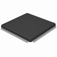
AT32UC3A364-ALUT Atmel, AT32UC3A364-ALUT Datasheet - Page 335

AT32UC3A364-ALUT
Manufacturer Part Number
AT32UC3A364-ALUT
Description
IC MCU 64KB FLASH 144LQFP
Manufacturer
Atmel
Series
AVR®32 UC3r
Specifications of AT32UC3A364-ALUT
Core Processor
AVR
Core Size
32-Bit
Speed
66MHz
Connectivity
EBI/EMI, I²C, IrDA, MMC, SPI, SSC, UART/USART, USB OTG
Peripherals
Brown-out Detect/Reset, DMA, POR, WDT
Number Of I /o
110
Program Memory Size
64KB (64K x 8)
Program Memory Type
FLASH
Ram Size
128K x 8
Voltage - Supply (vcc/vdd)
1.65 V ~ 1.95 V
Data Converters
A/D 8x10b
Oscillator Type
Internal
Operating Temperature
-40°C ~ 85°C
Package / Case
144-LQFP
Processor Series
AT32UC3x
Core
AVR32
Data Bus Width
32 bit
Data Ram Size
96 KB
Interface Type
IrDA/SCI/SCIF/UDI
Maximum Clock Frequency
66 MHz
Number Of Timers
3
Operating Supply Voltage
3 V to 3.6 V
Maximum Operating Temperature
+ 85 C
Mounting Style
SMD/SMT
3rd Party Development Tools
EWAVR32, EWAVR32-BL, KSK-EVK1100-PL
Development Tools By Supplier
ATAVRDRAGON, ATSTK500, ATSTK600, ATAVRISP2, ATAVRONEKIT, ATEXTWIFI, ATEVK1104
Minimum Operating Temperature
- 40 C
Controller Family/series
AT32UC3A
No. Of I/o's
110
Ram Memory Size
64KB
Cpu Speed
66MHz
No. Of Timers
2
Rohs Compliant
Yes
For Use With
ATEVK1104 - KIT DEV/EVAL FOR AVR32 AT32UC3AATAVRONEKIT - KIT AVR/AVR32 DEBUGGER/PROGRMMRATEVK1100 - KIT DEV/EVAL FOR AVR32 AT32UC3A
Lead Free Status / RoHS Status
Lead free / RoHS Compliant
Eeprom Size
-
Lead Free Status / Rohs Status
Lead free / RoHS Compliant
Available stocks
Company
Part Number
Manufacturer
Quantity
Price
- Current page: 335 of 1014
- Download datasheet (16Mb)
32072C–AVR32–2010/03
Note:
Note:
3. Write the starting source address in the SARx register for channel x.
4. Write the channel configuration information into the CFGx register for channel x.
5. Make sure that the LLI.CTLx register locations of all LLIs in memory (except the last)
6. Make sure that the LLI.LLPx register locations of all LLIs in memory (except the last)
7. Make sure that the LLI.DARx register location of all LLIs in memory point to the start
8. Make sure that the LLI.CTLx.DONE field of the LLI.CTLx register locations of all LLIs in
9. Clear any pending interrupts on the channel from the previous DMA transfer by writing
10. Program the CTLx, CFGx registers according to Row 7 as shown in
11. Program the LLPx register with LLPx(0), the pointer to the first Linked List item.
12. Finally, enable the channel by writing a ‘1’ to the ChEnReg.CH_EN bit. The transfer is
13. The DMACA fetches the first LLI from the location pointed to by LLPx(0).
14. Source and destination request single and burst DMACA transactions to transfer the
15.
16. The DMA transfer proceeds as follows:
a. Designate the handshaking interface type (hardware or software) for the source
b. If the hardware handshaking interface is activated for the source or destination
are set as shown in Row 7 of
last Linked List item must be set as described in Row 1 or Row 5 of
324.
are non-zero and point to the next Linked List Item.
destination block address proceeding that LLI fetch.
memory is cleared.
to the Interrupt Clear registers: ClearTfr, ClearBlock, ClearSrcTran, ClearDstTran,
ClearErr. Reading the Interrupt Raw Status and Interrupt Status registers confirms that
all interrupts have been cleared.
324.
performed. Make sure that bit 0 of the DmaCfgReg register is enabled.
block of data (assuming non-memory peripherals). DMACA acknowledges at the com-
pletion of every transaction (burst and single) in the block and carry out the block
transfer.
Table 19-1 on page
Hardware sets the block complete interrupt. The DMACA samples the row number as
shown in
fer has completed. Hardware sets the transfer complete interrupt and disables the
channel. You can either respond to the Block Complete or Transfer Complete interrupts,
or poll for the Channel Enable (ChEnReg.CH_EN) bit until it is cleared by hardware, to
detect when the transfer is complete. If the DMACA is not in Row 1 or 5 as shown in
Table 19-1 on page 324
a. If interrupts are enabled (CTLx.INT_EN = 1) and the block complete interrupt is un-
The values in the LLI.SARx register locations of each of the Linked List Items (LLIs) setup up in
memory, although fetched during a LLI fetch, are not used.
The LLI.SARx, LLI.DARx, LLI. LLPx and LLI.CTLx registers are fetched. The LLI.SARx register
although fetched is not used.
and destination peripherals. This is not required for memory. This step requires pro-
gramming the HS_SEL_SRC/HS_SEL_DST bits, respectively. Writing a ‘0’
activates the hardware handshaking interface to handle source/destination
requests for the specific channel. Writing a ‘1’ activates the software handshaking
interface source/destination requests.
peripheral, assign handshaking interface to the source and destination peripheral.
This requires programming the SRC_PER and DEST_PER bits, respectively.
masked (MaskBlock[x] = 1’b1, where x is the channel number) hardware sets the
Figure 19-7 on page 323
Table 19-1 on page
324The DMACA reloads the SARx register from the initial value.
the following steps are performed.
Table 19-1 on page 324
324. If the DMACA is in Row 1 or 5, then the DMA trans-
shows a Linked List example with two list items.
while the LLI.CTLx register of the
AT32UC3A3/A4
Table 19-1 on page
Table 19-1 on page
335
Related parts for AT32UC3A364-ALUT
Image
Part Number
Description
Manufacturer
Datasheet
Request
R

Part Number:
Description:
KIT DEV/EVAL FOR AT32UC3A3
Manufacturer:
Atmel
Datasheet:

Part Number:
Description:
DEV KIT FOR AVR/AVR32
Manufacturer:
Atmel
Datasheet:

Part Number:
Description:
INTERVAL AND WIPE/WASH WIPER CONTROL IC WITH DELAY
Manufacturer:
ATMEL Corporation
Datasheet:

Part Number:
Description:
Low-Voltage Voice-Switched IC for Hands-Free Operation
Manufacturer:
ATMEL Corporation
Datasheet:

Part Number:
Description:
MONOLITHIC INTEGRATED FEATUREPHONE CIRCUIT
Manufacturer:
ATMEL Corporation
Datasheet:

Part Number:
Description:
AM-FM Receiver IC U4255BM-M
Manufacturer:
ATMEL Corporation
Datasheet:

Part Number:
Description:
Monolithic Integrated Feature Phone Circuit
Manufacturer:
ATMEL Corporation
Datasheet:

Part Number:
Description:
Multistandard Video-IF and Quasi Parallel Sound Processing
Manufacturer:
ATMEL Corporation
Datasheet:

Part Number:
Description:
High-performance EE PLD
Manufacturer:
ATMEL Corporation
Datasheet:

Part Number:
Description:
8-bit Flash Microcontroller
Manufacturer:
ATMEL Corporation
Datasheet:

Part Number:
Description:
2-Wire Serial EEPROM
Manufacturer:
ATMEL Corporation
Datasheet:


