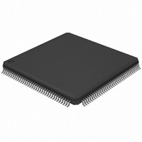
AT32UC3A364-ALUT Atmel, AT32UC3A364-ALUT Datasheet - Page 940

AT32UC3A364-ALUT
Manufacturer Part Number
AT32UC3A364-ALUT
Description
IC MCU 64KB FLASH 144LQFP
Manufacturer
Atmel
Series
AVR®32 UC3r
Specifications of AT32UC3A364-ALUT
Core Processor
AVR
Core Size
32-Bit
Speed
66MHz
Connectivity
EBI/EMI, I²C, IrDA, MMC, SPI, SSC, UART/USART, USB OTG
Peripherals
Brown-out Detect/Reset, DMA, POR, WDT
Number Of I /o
110
Program Memory Size
64KB (64K x 8)
Program Memory Type
FLASH
Ram Size
128K x 8
Voltage - Supply (vcc/vdd)
1.65 V ~ 1.95 V
Data Converters
A/D 8x10b
Oscillator Type
Internal
Operating Temperature
-40°C ~ 85°C
Package / Case
144-LQFP
Processor Series
AT32UC3x
Core
AVR32
Data Bus Width
32 bit
Data Ram Size
96 KB
Interface Type
IrDA/SCI/SCIF/UDI
Maximum Clock Frequency
66 MHz
Number Of Timers
3
Operating Supply Voltage
3 V to 3.6 V
Maximum Operating Temperature
+ 85 C
Mounting Style
SMD/SMT
3rd Party Development Tools
EWAVR32, EWAVR32-BL, KSK-EVK1100-PL
Development Tools By Supplier
ATAVRDRAGON, ATSTK500, ATSTK600, ATAVRISP2, ATAVRONEKIT, ATEXTWIFI, ATEVK1104
Minimum Operating Temperature
- 40 C
Controller Family/series
AT32UC3A
No. Of I/o's
110
Ram Memory Size
64KB
Cpu Speed
66MHz
No. Of Timers
2
Rohs Compliant
Yes
For Use With
ATEVK1104 - KIT DEV/EVAL FOR AVR32 AT32UC3AATAVRONEKIT - KIT AVR/AVR32 DEBUGGER/PROGRMMRATEVK1100 - KIT DEV/EVAL FOR AVR32 AT32UC3A
Lead Free Status / RoHS Status
Lead free / RoHS Compliant
Eeprom Size
-
Lead Free Status / Rohs Status
Lead free / RoHS Compliant
Available stocks
Company
Part Number
Manufacturer
Quantity
Price
- Current page: 940 of 1014
- Download datasheet (16Mb)
34.4.5.1
34.4.5.2
34.4.6
32072C–AVR32–2010/03
JTAG Interface
Power Management
Clocks
When an instruction that accesses the SAB is loaded in the instruction register, before entering
a sleep mode, the system clocks are not switched off to allow debugging in sleep modes. This
can lead to a program behaving differently when debugging.
The JTAG Interface uses the external TCK pin as clock source. This clock must be provided by
the JTAG master.
Instructions that use the SAB bus requires the internal main clock to be running.
The JTAG Interface is accessed through the dedicated JTAG pins shown in
939. The TMS control line navigates the TAP controller, as shown in
The TAP controller manages the serial access to the JTAG Instruction and Data registers. Data
is scanned into the selected instruction or data register on TDI, and out of the register on TDO,
in the Shift-IR and Shift-DR states, respectively. The LSB is shifted in and out first. TDO is high-
Z in other states than Shift-IR and Shift-DR.
The device implements a 5-bit Instruction Register (IR). A number of public JTAG instructions
defined by the JTAG standard are supported, as described in
ber of 32-bit AVR-specific private JTAG instructions described in
instruction selects a specific data register for the Shift-DR path, as described for each
instruction.
Section
AT32UC3A3/A4
Figure 34-5 on page
34.5.2, as well as a num-
Section
Table 34-6 on page
34.5.3. Each
941.
940
Related parts for AT32UC3A364-ALUT
Image
Part Number
Description
Manufacturer
Datasheet
Request
R

Part Number:
Description:
KIT DEV/EVAL FOR AT32UC3A3
Manufacturer:
Atmel
Datasheet:

Part Number:
Description:
DEV KIT FOR AVR/AVR32
Manufacturer:
Atmel
Datasheet:

Part Number:
Description:
INTERVAL AND WIPE/WASH WIPER CONTROL IC WITH DELAY
Manufacturer:
ATMEL Corporation
Datasheet:

Part Number:
Description:
Low-Voltage Voice-Switched IC for Hands-Free Operation
Manufacturer:
ATMEL Corporation
Datasheet:

Part Number:
Description:
MONOLITHIC INTEGRATED FEATUREPHONE CIRCUIT
Manufacturer:
ATMEL Corporation
Datasheet:

Part Number:
Description:
AM-FM Receiver IC U4255BM-M
Manufacturer:
ATMEL Corporation
Datasheet:

Part Number:
Description:
Monolithic Integrated Feature Phone Circuit
Manufacturer:
ATMEL Corporation
Datasheet:

Part Number:
Description:
Multistandard Video-IF and Quasi Parallel Sound Processing
Manufacturer:
ATMEL Corporation
Datasheet:

Part Number:
Description:
High-performance EE PLD
Manufacturer:
ATMEL Corporation
Datasheet:

Part Number:
Description:
8-bit Flash Microcontroller
Manufacturer:
ATMEL Corporation
Datasheet:

Part Number:
Description:
2-Wire Serial EEPROM
Manufacturer:
ATMEL Corporation
Datasheet:


