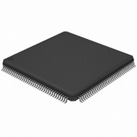
AT32UC3A364-ALUT Atmel, AT32UC3A364-ALUT Datasheet - Page 668

AT32UC3A364-ALUT
Manufacturer Part Number
AT32UC3A364-ALUT
Description
IC MCU 64KB FLASH 144LQFP
Manufacturer
Atmel
Series
AVR®32 UC3r
Specifications of AT32UC3A364-ALUT
Core Processor
AVR
Core Size
32-Bit
Speed
66MHz
Connectivity
EBI/EMI, I²C, IrDA, MMC, SPI, SSC, UART/USART, USB OTG
Peripherals
Brown-out Detect/Reset, DMA, POR, WDT
Number Of I /o
110
Program Memory Size
64KB (64K x 8)
Program Memory Type
FLASH
Ram Size
128K x 8
Voltage - Supply (vcc/vdd)
1.65 V ~ 1.95 V
Data Converters
A/D 8x10b
Oscillator Type
Internal
Operating Temperature
-40°C ~ 85°C
Package / Case
144-LQFP
Processor Series
AT32UC3x
Core
AVR32
Data Bus Width
32 bit
Data Ram Size
96 KB
Interface Type
IrDA/SCI/SCIF/UDI
Maximum Clock Frequency
66 MHz
Number Of Timers
3
Operating Supply Voltage
3 V to 3.6 V
Maximum Operating Temperature
+ 85 C
Mounting Style
SMD/SMT
3rd Party Development Tools
EWAVR32, EWAVR32-BL, KSK-EVK1100-PL
Development Tools By Supplier
ATAVRDRAGON, ATSTK500, ATSTK600, ATAVRISP2, ATAVRONEKIT, ATEXTWIFI, ATEVK1104
Minimum Operating Temperature
- 40 C
Controller Family/series
AT32UC3A
No. Of I/o's
110
Ram Memory Size
64KB
Cpu Speed
66MHz
No. Of Timers
2
Rohs Compliant
Yes
For Use With
ATEVK1104 - KIT DEV/EVAL FOR AVR32 AT32UC3AATAVRONEKIT - KIT AVR/AVR32 DEBUGGER/PROGRMMRATEVK1100 - KIT DEV/EVAL FOR AVR32 AT32UC3A
Lead Free Status / RoHS Status
Lead free / RoHS Compliant
Eeprom Size
-
Lead Free Status / Rohs Status
Lead free / RoHS Compliant
Available stocks
Company
Part Number
Manufacturer
Quantity
Price
- Current page: 668 of 1014
- Download datasheet (16Mb)
32072C–AVR32–2010/03
•Programming example for multi-block dma transfer : run and link at end of buffer
•Programming example for multi-block dma transfer : load next descriptor now
The idea is to run first a single block transfer followed automatically by a linked list of DMA. The
following sequence may be used:
The UDDMAnSTATUS.CHEN bit is set indicating that the dma channel is enable.
As soon as an OUT packet is stored inside the endpoint, the UDDMAnSTATUS.CHACTIVE bit
is set to one, indicating that the DMA channel is transfering data from the endpoint to the desti-
nation address until the endpoint is empty or the channel byte length is reached. Once the
endpoint is empty, the UDDMAnSTATUS.CHACTIVE bit is cleared.
Once the first DMA channel is completed (i.e : the channel byte length is reached), after one or
multiple processed OUT packet, the UDDMAnCONTROL.CHEN bit is cleared. As a conse-
q u e n c e ,
UDDMAnSTATUS.EOCHBUFFSTA bit is set indicating a end of dma channel. If the UDDMAn-
CONTROL.DMAENDEN bit was set, the last endpoint bank will be properly released even if
there are some residual datas inside, i.e: OUT packet truncation at the end of DMA buffer when
the dma channel byte lenght is not an integral multiple of the endpoint size. Note that the
UDDMAnCONTROL.LDNXTCH bit remains to one indicating that a linked descriptor will be
loaded.
Once the new descriptor is loaded from the UDDMAnNEXTDESC memory address, the UDDM-
AnSTATUS.DESCLDSTA bit is set, and the UDDMAnCONTROL register is updated from the
memory. As a consequence, the UDDMAnSTATUS.CHEN bit is set, and the UDDMAnSTA-
TUS.CHACTIVE is set as soon as the endpoint is ready to be sourced by the DMA (received
OUT data packet).
This sequence is repeated until a last linked descriptor is processed. The last descriptor is
detected according to row 2 as shown in
At the end of the last descriptor, the UDDMAnCONTROL.CHEN bit is cleared. As a conse-
quence, after a few cycles latency, the UDDMAnSTATUS.CHEN bit is also cleared.
The idea is to directly run first a linked list of DMA. The following sequence may be used: The
following sequence may be used:
• Configure the targerted endpoint (source) as OUT type, and set the automatic bank switching
• Set up the chain of linked list of descripor in memory. Each descriptor is composed of 3 items
• Write the starting destination address in the UDDMAnADDR register.
• Program the UDDMAnNEXTDESC register.
• Program the channel byte length in the UDDMAnCONTROL register.
• Optionnaly set the BUFFCLOSEINEN bit in the UDDMAnCONTROL register.
• Program the UDDMAnCONTROL according to Row 4 as shown in
• Configure the targerted endpoint (source) as OUT type, and set the automatic bank switching
for this endpoint in the UECFGn register to handle multiple OUT packet.
: channel next descriptor address, channel destination address and channel control. The last
descriptor should be programmed according to row 2 as shown in
for this endpoint in the UECFGn register to handle multiple OUT packet.
t h e
U D D M A n S T A T U S . C H E N
Figure 26-7 on page
b i t
i s
720.
a l s o
AT32UC3A3/A4
Figure 26-7 on page
Figure 26-7 on page
c l e a r e d ,
a n d
720.
720.
668
t h e
Related parts for AT32UC3A364-ALUT
Image
Part Number
Description
Manufacturer
Datasheet
Request
R

Part Number:
Description:
KIT DEV/EVAL FOR AT32UC3A3
Manufacturer:
Atmel
Datasheet:

Part Number:
Description:
DEV KIT FOR AVR/AVR32
Manufacturer:
Atmel
Datasheet:

Part Number:
Description:
INTERVAL AND WIPE/WASH WIPER CONTROL IC WITH DELAY
Manufacturer:
ATMEL Corporation
Datasheet:

Part Number:
Description:
Low-Voltage Voice-Switched IC for Hands-Free Operation
Manufacturer:
ATMEL Corporation
Datasheet:

Part Number:
Description:
MONOLITHIC INTEGRATED FEATUREPHONE CIRCUIT
Manufacturer:
ATMEL Corporation
Datasheet:

Part Number:
Description:
AM-FM Receiver IC U4255BM-M
Manufacturer:
ATMEL Corporation
Datasheet:

Part Number:
Description:
Monolithic Integrated Feature Phone Circuit
Manufacturer:
ATMEL Corporation
Datasheet:

Part Number:
Description:
Multistandard Video-IF and Quasi Parallel Sound Processing
Manufacturer:
ATMEL Corporation
Datasheet:

Part Number:
Description:
High-performance EE PLD
Manufacturer:
ATMEL Corporation
Datasheet:

Part Number:
Description:
8-bit Flash Microcontroller
Manufacturer:
ATMEL Corporation
Datasheet:

Part Number:
Description:
2-Wire Serial EEPROM
Manufacturer:
ATMEL Corporation
Datasheet:


