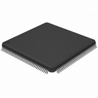
AT32UC3A364-ALUT Atmel, AT32UC3A364-ALUT Datasheet - Page 513

AT32UC3A364-ALUT
Manufacturer Part Number
AT32UC3A364-ALUT
Description
IC MCU 64KB FLASH 144LQFP
Manufacturer
Atmel
Series
AVR®32 UC3r
Specifications of AT32UC3A364-ALUT
Core Processor
AVR
Core Size
32-Bit
Speed
66MHz
Connectivity
EBI/EMI, I²C, IrDA, MMC, SPI, SSC, UART/USART, USB OTG
Peripherals
Brown-out Detect/Reset, DMA, POR, WDT
Number Of I /o
110
Program Memory Size
64KB (64K x 8)
Program Memory Type
FLASH
Ram Size
128K x 8
Voltage - Supply (vcc/vdd)
1.65 V ~ 1.95 V
Data Converters
A/D 8x10b
Oscillator Type
Internal
Operating Temperature
-40°C ~ 85°C
Package / Case
144-LQFP
Processor Series
AT32UC3x
Core
AVR32
Data Bus Width
32 bit
Data Ram Size
96 KB
Interface Type
IrDA/SCI/SCIF/UDI
Maximum Clock Frequency
66 MHz
Number Of Timers
3
Operating Supply Voltage
3 V to 3.6 V
Maximum Operating Temperature
+ 85 C
Mounting Style
SMD/SMT
3rd Party Development Tools
EWAVR32, EWAVR32-BL, KSK-EVK1100-PL
Development Tools By Supplier
ATAVRDRAGON, ATSTK500, ATSTK600, ATAVRISP2, ATAVRONEKIT, ATEXTWIFI, ATEVK1104
Minimum Operating Temperature
- 40 C
Controller Family/series
AT32UC3A
No. Of I/o's
110
Ram Memory Size
64KB
Cpu Speed
66MHz
No. Of Timers
2
Rohs Compliant
Yes
For Use With
ATEVK1104 - KIT DEV/EVAL FOR AVR32 AT32UC3AATAVRONEKIT - KIT AVR/AVR32 DEBUGGER/PROGRMMRATEVK1100 - KIT DEV/EVAL FOR AVR32 AT32UC3A
Lead Free Status / RoHS Status
Lead free / RoHS Compliant
Eeprom Size
-
Lead Free Status / Rohs Status
Lead free / RoHS Compliant
Available stocks
Company
Part Number
Manufacturer
Quantity
Price
- Current page: 513 of 1014
- Download datasheet (16Mb)
24.7.5
24.7.5.1
24.7.5.2
32072C–AVR32–2010/03
Frame Sync
Frame sync data
Frame sync edge detection
The transmitter and receiver frame synchro pins, TX_FRAME_SYNC and RX_FRAME_SYNC,
can be programmed to generate different kinds of frame synchronization signals. The
RFMR.FSOS and TFMR.FSOS fields are used to select the required waveform.
If a pulse waveform is selected, in reception, the Receive Frame Sync Length High Part and the
Receive Frame Sync Length fields in the RFMR register (RFMR.FSLENHI and RFMR.FSLEN)
define the length of the pulse, from 1 bit time up to 256 bit time.
Similarly, in transmission, the Transmit Frame Sync Length High Part and the Transmit Frame
Sync Length fields in the TFMR register (TFMR.FSLENHI and TFMR.FSLEN) define the length
of the pulse, from 1 bit up to 256 bit time.
The periodicity of the RX_FRAME_SYNC and TX_FRAME_SYNC pulse outputs can be config-
ured respectively through the Receive Period Divider Selection field in the RCMR register
(RCMR.PERIOD) and the Transmit Period Divider Selection field in the TCMR register
(TCMR.PERIOD).
Frame Sync Data transmits or receives a specific tag during the Frame Sync signal.
During the Frame Sync signal, the receiver can sample the RX_DATA line and store the data in
the Receive Sync Holding Register (RSHR) and the transmitter can transfer the Transmit Sync
Holding Register (TSHR) in the shifter register.
The data length to be sampled in reception during the Frame Sync signal shall be written to the
RFMR.FSLENHI and RFMR.FSLEN fields.
The data length to be shifted out in transmission during the Frame Sync signal shall be written to
the TFMR.FSLENHI and TFMR.FSLEN fields.
Concerning the Receive Frame Sync Data operation, if the Frame Sync Length is equal to or
lower than the delay between the start event and the actual data reception, the data sampling
operation is performed in the RSHR through the receive shift register.
The Transmit Frame Sync operation is performed by the transmitter only if the Frame Sync Data
Enable bit in TFMR register (TFMR.FSDEN) is written to one. If the Frame Sync length is equal
to or lower than the delay between the start event and the actual data transmission, the normal
transmission has priority and the data contained in the TSHR is transferred in the transmit regis-
ter, then shifted out.
The Frame Sync Edge detection is configured by writing to the Frame Sync Edge Detection bit in
the RFMR/TFMR registers (RFMR.FSEDGE and TFMR.FSEDGE). This sets the Receive Sync
• Programmable low or high levels during data transfer are supported.
• Programmable high levels before the start of data transfers or toggling are also supported.
Transmission Pulse Length
Reception Pulse Length
=
=
((16
((16
×
×
FSLENHI
FSLENHI
)
)
+
+
FSLEN
FSLEN
+
+
1) receive clock periods
1) transmit clock periods
AT32UC3A3/A4
513
Related parts for AT32UC3A364-ALUT
Image
Part Number
Description
Manufacturer
Datasheet
Request
R

Part Number:
Description:
KIT DEV/EVAL FOR AT32UC3A3
Manufacturer:
Atmel
Datasheet:

Part Number:
Description:
DEV KIT FOR AVR/AVR32
Manufacturer:
Atmel
Datasheet:

Part Number:
Description:
INTERVAL AND WIPE/WASH WIPER CONTROL IC WITH DELAY
Manufacturer:
ATMEL Corporation
Datasheet:

Part Number:
Description:
Low-Voltage Voice-Switched IC for Hands-Free Operation
Manufacturer:
ATMEL Corporation
Datasheet:

Part Number:
Description:
MONOLITHIC INTEGRATED FEATUREPHONE CIRCUIT
Manufacturer:
ATMEL Corporation
Datasheet:

Part Number:
Description:
AM-FM Receiver IC U4255BM-M
Manufacturer:
ATMEL Corporation
Datasheet:

Part Number:
Description:
Monolithic Integrated Feature Phone Circuit
Manufacturer:
ATMEL Corporation
Datasheet:

Part Number:
Description:
Multistandard Video-IF and Quasi Parallel Sound Processing
Manufacturer:
ATMEL Corporation
Datasheet:

Part Number:
Description:
High-performance EE PLD
Manufacturer:
ATMEL Corporation
Datasheet:

Part Number:
Description:
8-bit Flash Microcontroller
Manufacturer:
ATMEL Corporation
Datasheet:

Part Number:
Description:
2-Wire Serial EEPROM
Manufacturer:
ATMEL Corporation
Datasheet:


