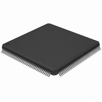
AT32UC3A364-ALUT Atmel, AT32UC3A364-ALUT Datasheet - Page 405

AT32UC3A364-ALUT
Manufacturer Part Number
AT32UC3A364-ALUT
Description
IC MCU 64KB FLASH 144LQFP
Manufacturer
Atmel
Series
AVR®32 UC3r
Specifications of AT32UC3A364-ALUT
Core Processor
AVR
Core Size
32-Bit
Speed
66MHz
Connectivity
EBI/EMI, I²C, IrDA, MMC, SPI, SSC, UART/USART, USB OTG
Peripherals
Brown-out Detect/Reset, DMA, POR, WDT
Number Of I /o
110
Program Memory Size
64KB (64K x 8)
Program Memory Type
FLASH
Ram Size
128K x 8
Voltage - Supply (vcc/vdd)
1.65 V ~ 1.95 V
Data Converters
A/D 8x10b
Oscillator Type
Internal
Operating Temperature
-40°C ~ 85°C
Package / Case
144-LQFP
Processor Series
AT32UC3x
Core
AVR32
Data Bus Width
32 bit
Data Ram Size
96 KB
Interface Type
IrDA/SCI/SCIF/UDI
Maximum Clock Frequency
66 MHz
Number Of Timers
3
Operating Supply Voltage
3 V to 3.6 V
Maximum Operating Temperature
+ 85 C
Mounting Style
SMD/SMT
3rd Party Development Tools
EWAVR32, EWAVR32-BL, KSK-EVK1100-PL
Development Tools By Supplier
ATAVRDRAGON, ATSTK500, ATSTK600, ATAVRISP2, ATAVRONEKIT, ATEXTWIFI, ATEVK1104
Minimum Operating Temperature
- 40 C
Controller Family/series
AT32UC3A
No. Of I/o's
110
Ram Memory Size
64KB
Cpu Speed
66MHz
No. Of Timers
2
Rohs Compliant
Yes
For Use With
ATEVK1104 - KIT DEV/EVAL FOR AVR32 AT32UC3AATAVRONEKIT - KIT AVR/AVR32 DEBUGGER/PROGRMMRATEVK1100 - KIT DEV/EVAL FOR AVR32 AT32UC3A
Lead Free Status / RoHS Status
Lead free / RoHS Compliant
Eeprom Size
-
Lead Free Status / Rohs Status
Lead free / RoHS Compliant
Available stocks
Company
Part Number
Manufacturer
Quantity
Price
- Current page: 405 of 1014
- Download datasheet (16Mb)
Figure 21-4. SPI Transfer Format (NCPHA = 0, 8 bits per transfer)
21.7.3
32072C–AVR32–2010/03
SPCK cycle (for reference)
Master Mode Operations
(from master)
(from slave)
(CPOL = 0)
(CPOL = 1)
(to slave)
SPCK
SPCK
MOSI
MISO
NSS
When configured in master mode, the SPI uses the internal programmable baud rate generator
as clock source. It fully controls the data transfers to and from the slave(s) connected to the SPI
bus. The SPI drives the chip select line to the slave and the serial clock signal (SPCK).
The SPI features two holding registers, the Transmit Data Register (TDR) and the Receive Data
Register (RDR), and a single Shift Register. The holding registers maintain the data flow at a
constant rate.
After enabling the SPI, a data transfer begins when the processor writes to the TDR register.
The written data is immediately transferred in the Shift Register and transfer on the SPI bus
starts. While the data in the Shift Register is shifted on the MOSI line, the MISO line is sampled
and shifted in the Shift Register. Transmission cannot occur without reception.
Before writing to the TDR, the Peripheral Chip Select field in TDR (TDR.PCS) must be written in
order to select a slave.
If new data is written to TDR during the transfer, it stays in it until the current transfer is com-
pleted. Then, the received data is transferred from the Shift Register to RDR, the data in TDR is
loaded in the Shift Register and a new transfer starts.
The transfer of a data written in TDR in the Shift Register is indicated by the Transmit Data Reg-
ister Empty bit in the Status Register (SR.TDRE). When new data is written in TDR, this bit is
cleared. The SR.TDRE bit is used to trigger the Transmit Peripheral DMA Controller channel.
The end of transfer is indicated by the Transmission Registers Empty bit in the SR register
(SR.TXEMPTY). If a transfer delay (CSRn.DLYBCT) is greater than zero for the last transfer,
SR.TXEMPTY is set after the completion of said delay. The CLK_SPI can be switched off at this
time.
During reception, received data are transferred from the Shift Register to the reception FIFO.
The FIFO can contain up to 4 characters (both Receive Data and Peripheral Chip Select fields).
While a character of the FIFO is unread, the Receive Data Register Full bit in SR remains high
(SR.RDRF). Characters are read through the RDR register. If the four characters stored in the
FIFO are not read and if a new character is stored, this sets the Overrun Error Status bit in the
SR register (SR.OVRES). The procedure to follow in such a case is described in
21.7.3.8.
***
1
*** Not Defined, but normaly LSB of previous character transmitted
MSB
MSB
2
6
6
3
5
5
4
4
4
5
3
3
6
2
2
7
1
1
8
LSB
AT32UC3A3/A4
LSB
Section
405
Related parts for AT32UC3A364-ALUT
Image
Part Number
Description
Manufacturer
Datasheet
Request
R

Part Number:
Description:
KIT DEV/EVAL FOR AT32UC3A3
Manufacturer:
Atmel
Datasheet:

Part Number:
Description:
DEV KIT FOR AVR/AVR32
Manufacturer:
Atmel
Datasheet:

Part Number:
Description:
INTERVAL AND WIPE/WASH WIPER CONTROL IC WITH DELAY
Manufacturer:
ATMEL Corporation
Datasheet:

Part Number:
Description:
Low-Voltage Voice-Switched IC for Hands-Free Operation
Manufacturer:
ATMEL Corporation
Datasheet:

Part Number:
Description:
MONOLITHIC INTEGRATED FEATUREPHONE CIRCUIT
Manufacturer:
ATMEL Corporation
Datasheet:

Part Number:
Description:
AM-FM Receiver IC U4255BM-M
Manufacturer:
ATMEL Corporation
Datasheet:

Part Number:
Description:
Monolithic Integrated Feature Phone Circuit
Manufacturer:
ATMEL Corporation
Datasheet:

Part Number:
Description:
Multistandard Video-IF and Quasi Parallel Sound Processing
Manufacturer:
ATMEL Corporation
Datasheet:

Part Number:
Description:
High-performance EE PLD
Manufacturer:
ATMEL Corporation
Datasheet:

Part Number:
Description:
8-bit Flash Microcontroller
Manufacturer:
ATMEL Corporation
Datasheet:

Part Number:
Description:
2-Wire Serial EEPROM
Manufacturer:
ATMEL Corporation
Datasheet:


