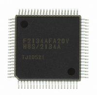
DF2134AFA20V Renesas Electronics America, DF2134AFA20V Datasheet - Page 512

DF2134AFA20V
Manufacturer Part Number
DF2134AFA20V
Description
IC H8S/2100 MCU FLASH 80QFP
Manufacturer
Renesas Electronics America
Series
H8® H8S/2100r
Datasheets
1.HEWH8E10A.pdf
(19 pages)
2.D12312SVTE25V.pdf
(341 pages)
3.DF2134AFA20V.pdf
(1063 pages)
Specifications of DF2134AFA20V
Core Processor
H8S/2000
Core Size
16-Bit
Speed
20MHz
Connectivity
IrDA, SCI
Peripherals
POR, PWM, WDT
Number Of I /o
58
Program Memory Size
128KB (128K x 8)
Program Memory Type
FLASH
Ram Size
4K x 8
Voltage - Supply (vcc/vdd)
4 V ~ 5.5 V
Data Converters
A/D 8x10b; D/A 2x8b
Oscillator Type
Internal
Operating Temperature
-20°C ~ 75°C
Package / Case
80-QFP
For Use With
3DK2166 - DEV EVAL KIT H8S/2166
Lead Free Status / RoHS Status
Lead free / RoHS Compliant
Eeprom Size
-
Available stocks
Company
Part Number
Manufacturer
Quantity
Price
Company:
Part Number:
DF2134AFA20V
Manufacturer:
Renesas Electronics America
Quantity:
10 000
- Current page: 512 of 1063
- Download datasheet (6Mb)
Section 16 I
16.1.2
Figure 16.1 shows a block diagram of the I
Figure 16.2 shows an example of I/O pin connections to external circuits. Channel 0 I/O pins and
channel 1 I/O pins differ in structure, and have different specifications for permissible applied
voltages. For details, see section 25, Electrical Characteristics.
Rev. 4.00 Jun 06, 2006 page 456 of 1004
REJ09B0301-0400
Wait function in slave mode (I
A wait request can be generated by driving the SCL pin low after data transfer, excluding
acknowledgement. The wait request is cleared when the next transfer becomes possible.
Three interrupt sources
Selection of 16 internal clocks (in master mode)
Direct bus drive (with SCL and SDA pins)
Automatic switching from formatless mode to I
Data transfer end (including transmission mode transition with I
reception after loss of master arbitration)
Address match: when any slave address matches or the general call address is received in
slave receive mode (I
Stop condition detection
Two pins—P52/SCL0 and P97/SDA0—(normally NMOS push-pull outputs) function as
NMOS open-drain outputs when the bus drive function is selected.
Two pins—P86/SCL1 and P42/SDA1—(normally CMOS pins) function as NMOS-only
outputs when the bus drive function is selected.
Formatless operation (no start/stop conditions, non-addressing mode) in slave mode
Operation using a common data pin (SDA) and independent clock pins (VSYNCI, SCL)
Automatic switching from formatless mode to I
Block Diagram
2
C Bus Interface [H8S/2138 Group Option]
2
C bus format)
2
C bus format)
2
C bus interface.
2
C bus format (channel 0 only)
2
C bus format on the fall of the SCL pin
2
C bus format and address
Related parts for DF2134AFA20V
Image
Part Number
Description
Manufacturer
Datasheet
Request
R

Part Number:
Description:
KIT STARTER FOR M16C/29
Manufacturer:
Renesas Electronics America
Datasheet:

Part Number:
Description:
KIT STARTER FOR R8C/2D
Manufacturer:
Renesas Electronics America
Datasheet:

Part Number:
Description:
R0K33062P STARTER KIT
Manufacturer:
Renesas Electronics America
Datasheet:

Part Number:
Description:
KIT STARTER FOR R8C/23 E8A
Manufacturer:
Renesas Electronics America
Datasheet:

Part Number:
Description:
KIT STARTER FOR R8C/25
Manufacturer:
Renesas Electronics America
Datasheet:

Part Number:
Description:
KIT STARTER H8S2456 SHARPE DSPLY
Manufacturer:
Renesas Electronics America
Datasheet:

Part Number:
Description:
KIT STARTER FOR R8C38C
Manufacturer:
Renesas Electronics America
Datasheet:

Part Number:
Description:
KIT STARTER FOR R8C35C
Manufacturer:
Renesas Electronics America
Datasheet:

Part Number:
Description:
KIT STARTER FOR R8CL3AC+LCD APPS
Manufacturer:
Renesas Electronics America
Datasheet:

Part Number:
Description:
KIT STARTER FOR RX610
Manufacturer:
Renesas Electronics America
Datasheet:

Part Number:
Description:
KIT STARTER FOR R32C/118
Manufacturer:
Renesas Electronics America
Datasheet:

Part Number:
Description:
KIT DEV RSK-R8C/26-29
Manufacturer:
Renesas Electronics America
Datasheet:

Part Number:
Description:
KIT STARTER FOR SH7124
Manufacturer:
Renesas Electronics America
Datasheet:

Part Number:
Description:
KIT STARTER FOR H8SX/1622
Manufacturer:
Renesas Electronics America
Datasheet:

Part Number:
Description:
KIT DEV FOR SH7203
Manufacturer:
Renesas Electronics America
Datasheet:


