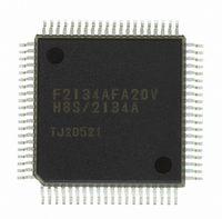
DF2134AFA20V Renesas Electronics America, DF2134AFA20V Datasheet - Page 41

DF2134AFA20V
Manufacturer Part Number
DF2134AFA20V
Description
IC H8S/2100 MCU FLASH 80QFP
Manufacturer
Renesas Electronics America
Series
H8® H8S/2100r
Datasheets
1.HEWH8E10A.pdf
(19 pages)
2.D12312SVTE25V.pdf
(341 pages)
3.DF2134AFA20V.pdf
(1063 pages)
Specifications of DF2134AFA20V
Core Processor
H8S/2000
Core Size
16-Bit
Speed
20MHz
Connectivity
IrDA, SCI
Peripherals
POR, PWM, WDT
Number Of I /o
58
Program Memory Size
128KB (128K x 8)
Program Memory Type
FLASH
Ram Size
4K x 8
Voltage - Supply (vcc/vdd)
4 V ~ 5.5 V
Data Converters
A/D 8x10b; D/A 2x8b
Oscillator Type
Internal
Operating Temperature
-20°C ~ 75°C
Package / Case
80-QFP
For Use With
3DK2166 - DEV EVAL KIT H8S/2166
Lead Free Status / RoHS Status
Lead free / RoHS Compliant
Eeprom Size
-
Available stocks
Company
Part Number
Manufacturer
Quantity
Price
Company:
Part Number:
DF2134AFA20V
Manufacturer:
Renesas Electronics America
Quantity:
10 000
- Current page: 41 of 1063
- Download datasheet (6Mb)
Figure 12.10
Figure 12.11
Figure 12.12
Figure 12.13
Figure 12.14
Figure 12.15
Section 13 Timer Connection [H8S/2138 Group]
Figure 13.1
Figure 13.2
Figure 13.3
Figure 13.4
Figure 13.5
Figure 13.6
Figure 13.7
Figure 13.8
Figure 13.9
Section 14 Watchdog Timer (WDT)
Figure 14.1 (a) Block Diagram of WDT0 .................................................................................. 372
Figure 14.1 (b) Block Diagram of WDT1 .................................................................................. 373
Figure 14.2
Figure 14.3
Figure 14.4
Figure 14.5
Figure 14.6
Section 15 Serial Communication Interface (SCI, IrDA)
Figure 15.1
Figure 15.2
Figure 15.3
Figure 15.4
Figure 15.5
Figure 15.6
Figure 15.7
Timing of Input Capture Signal (When Input Capture Input Signal Enters
while TICRR and TICRF Are Being Read)....................................................... 331
Switching of Input Capture Signal .................................................................... 331
Pulse Output (Example) .................................................................................... 334
Contention between TCNT Write and Clear ..................................................... 335
Contention between TCNT Write and Increment.............................................. 336
Contention between TCOR Write and Compare-Match.................................... 337
Block Diagram of Timer Connection Facility ................................................... 342
Timing Chart for PWM Decoding..................................................................... 356
Timing Chart for Clamp Waveform Generation (CL1 and CL2 Signals) ......... 358
Timing Chart for Clamp Waveform Generation (CL3 Signal).......................... 358
Timing Chart for Measurement of IVI Signal and IHI Signal Divided
Waveform Periods ............................................................................................. 360
2fH Modification Timing Chart ........................................................................ 361
Fall Modification/IHI Synchronization Timing Chart....................................... 363
IVG Signal/IHG Signal/CL4 Signal Timing Chart............................................ 366
CBLANK Output Waveform Generation .......................................................... 369
Format of Data Written to TCNT and TCSR (Example of WDT0) .................. 380
Operation in Watchdog Timer Mode................................................................. 382
Operation in Interval Timer Mode..................................................................... 383
Timing of OVF Setting...................................................................................... 383
Contention between TCNT Write and Increment.............................................. 384
Block Diagram of SCI ....................................................................................... 389
Data Format in Asynchronous Communication
(Example with 8-Bit Data, Parity, Two Stop Bits) ............................................ 419
Relation between Output Clock and Transfer Data Phase
(Asynchronous Mode) ....................................................................................... 421
Sample SCI Initialization Flowchart ................................................................. 422
Sample Serial Transmission Flowchart ............................................................. 423
Example of Operation in Transmission in Asynchronous Mode
(Example with 8-Bit Data, Parity, One Stop Bit) .............................................. 425
Sample Serial Reception Data Flowchart .......................................................... 426
Rev. 4.00 Jun 06, 2006 page xxxix of liv
Related parts for DF2134AFA20V
Image
Part Number
Description
Manufacturer
Datasheet
Request
R

Part Number:
Description:
KIT STARTER FOR M16C/29
Manufacturer:
Renesas Electronics America
Datasheet:

Part Number:
Description:
KIT STARTER FOR R8C/2D
Manufacturer:
Renesas Electronics America
Datasheet:

Part Number:
Description:
R0K33062P STARTER KIT
Manufacturer:
Renesas Electronics America
Datasheet:

Part Number:
Description:
KIT STARTER FOR R8C/23 E8A
Manufacturer:
Renesas Electronics America
Datasheet:

Part Number:
Description:
KIT STARTER FOR R8C/25
Manufacturer:
Renesas Electronics America
Datasheet:

Part Number:
Description:
KIT STARTER H8S2456 SHARPE DSPLY
Manufacturer:
Renesas Electronics America
Datasheet:

Part Number:
Description:
KIT STARTER FOR R8C38C
Manufacturer:
Renesas Electronics America
Datasheet:

Part Number:
Description:
KIT STARTER FOR R8C35C
Manufacturer:
Renesas Electronics America
Datasheet:

Part Number:
Description:
KIT STARTER FOR R8CL3AC+LCD APPS
Manufacturer:
Renesas Electronics America
Datasheet:

Part Number:
Description:
KIT STARTER FOR RX610
Manufacturer:
Renesas Electronics America
Datasheet:

Part Number:
Description:
KIT STARTER FOR R32C/118
Manufacturer:
Renesas Electronics America
Datasheet:

Part Number:
Description:
KIT DEV RSK-R8C/26-29
Manufacturer:
Renesas Electronics America
Datasheet:

Part Number:
Description:
KIT STARTER FOR SH7124
Manufacturer:
Renesas Electronics America
Datasheet:

Part Number:
Description:
KIT STARTER FOR H8SX/1622
Manufacturer:
Renesas Electronics America
Datasheet:

Part Number:
Description:
KIT DEV FOR SH7203
Manufacturer:
Renesas Electronics America
Datasheet:


