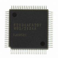
DF2134AFA20V Renesas Electronics America, DF2134AFA20V Datasheet - Page 39

DF2134AFA20V
Manufacturer Part Number
DF2134AFA20V
Description
IC H8S/2100 MCU FLASH 80QFP
Manufacturer
Renesas Electronics America
Series
H8® H8S/2100r
Datasheets
1.HEWH8E10A.pdf
(19 pages)
2.D12312SVTE25V.pdf
(341 pages)
3.DF2134AFA20V.pdf
(1063 pages)
Specifications of DF2134AFA20V
Core Processor
H8S/2000
Core Size
16-Bit
Speed
20MHz
Connectivity
IrDA, SCI
Peripherals
POR, PWM, WDT
Number Of I /o
58
Program Memory Size
128KB (128K x 8)
Program Memory Type
FLASH
Ram Size
4K x 8
Voltage - Supply (vcc/vdd)
4 V ~ 5.5 V
Data Converters
A/D 8x10b; D/A 2x8b
Oscillator Type
Internal
Operating Temperature
-20°C ~ 75°C
Package / Case
80-QFP
For Use With
3DK2166 - DEV EVAL KIT H8S/2166
Lead Free Status / RoHS Status
Lead free / RoHS Compliant
Eeprom Size
-
Available stocks
Company
Part Number
Manufacturer
Quantity
Price
Company:
Part Number:
DF2134AFA20V
Manufacturer:
Renesas Electronics America
Quantity:
10 000
- Current page: 39 of 1063
- Download datasheet (6Mb)
Figure 7.4
Figure 7.5
Figure 7.6
Figure 7.7
Figure 7.8
Figure 7.9
Figure 7.10
Figure 7.11
Figure 7.12
Section 8 I/O Ports
Figure 8.1
Figure 8.2
Figure 8.3
Figure 8.4
Figure 8.5
Figure 8.6
Figure 8.7
Figure 8.8
Figure 8.9
Figure 8.10
Figure 8.11
Figure 8.12
Figure 8.13
Figure 8.14
Figure 8.15
Figure 8.16
Figure 8.17
Section 9 8-Bit PWM Timers [H8S/2138 Group]
Figure 9.1
Figure 9.2
Section 10 14-Bit PWM D/A
Figure 10.1
Figure 10.2 (a) Access to DACNT (CPU Writes H'AA57 to DACNT) ..................................... 263
Figure 10.2 (b) Access to DACNT (CPU Reads H'AA57 from DACNT) ................................. 264
Figure 10.3
Figure 10.4 (1) Output Waveform.............................................................................................. 267
Figure 10.4 (2) Output Waveform.............................................................................................. 267
Correspondence between DTC Vector Address and Register Information ....... 173
Location of DTC Register Information in Address Space................................. 175
Memory Mapping in Normal Mode .................................................................. 176
Memory Mapping in Repeat Mode.................................................................... 177
Memory Mapping in Block Transfer Mode....................................................... 179
Memory Mapping in Chain Transfer ................................................................. 180
DTC Operation Timing (Normal Mode or Repeat Mode)................................. 181
DTC Operation Timing (Block Transfer Mode, with Block Size of 2)............. 181
DTC Operation Timing (Chain Transfer).......................................................... 182
Port 1 Pin Functions .......................................................................................... 196
Port 1 Pin Functions (Mode 1) .......................................................................... 199
Port 1 Pin Functions (Modes 2 and 3 (EXPE = 1)) ........................................... 199
Port 1 Pin Functions (Modes 2 and 3 (EXPE = 0)) ........................................... 200
Port 2 Pin Functions .......................................................................................... 202
Port 2 Pin Functions (Mode 1) .......................................................................... 205
Port 2 Pin Functions (Modes 2 and 3 (EXPE = 1)) ........................................... 206
Port 2 Pin Functions (Modes 2 and 3 (EXPE = 0)) ........................................... 206
Port 3 Pin Functions .......................................................................................... 208
Port 3 Pin Functions (Modes 1, 2, and 3 (EXPE = 1)) ...................................... 211
Port 3 Pin Functions (Modes 2 and 3 (EXPE = 0)) ........................................... 211
Port 4 Pin Functions .......................................................................................... 213
Port 5 Pin Functions .......................................................................................... 218
Port 6 Pin Functions .......................................................................................... 221
Port 7 Pin Functions .......................................................................................... 228
Port 8 Pin Functions .......................................................................................... 230
Port 9 Pin Functions .......................................................................................... 234
Block Diagram of PWM Timer Module............................................................ 242
Example of Additional Pulse Timing
(When Upper 4 Bits of PWDR = 1000)............................................................. 252
PWM D/A Block Diagram ................................................................................ 254
PWM D/A Operation......................................................................................... 265
Rev. 4.00 Jun 06, 2006 page xxxvii of liv
Related parts for DF2134AFA20V
Image
Part Number
Description
Manufacturer
Datasheet
Request
R

Part Number:
Description:
KIT STARTER FOR M16C/29
Manufacturer:
Renesas Electronics America
Datasheet:

Part Number:
Description:
KIT STARTER FOR R8C/2D
Manufacturer:
Renesas Electronics America
Datasheet:

Part Number:
Description:
R0K33062P STARTER KIT
Manufacturer:
Renesas Electronics America
Datasheet:

Part Number:
Description:
KIT STARTER FOR R8C/23 E8A
Manufacturer:
Renesas Electronics America
Datasheet:

Part Number:
Description:
KIT STARTER FOR R8C/25
Manufacturer:
Renesas Electronics America
Datasheet:

Part Number:
Description:
KIT STARTER H8S2456 SHARPE DSPLY
Manufacturer:
Renesas Electronics America
Datasheet:

Part Number:
Description:
KIT STARTER FOR R8C38C
Manufacturer:
Renesas Electronics America
Datasheet:

Part Number:
Description:
KIT STARTER FOR R8C35C
Manufacturer:
Renesas Electronics America
Datasheet:

Part Number:
Description:
KIT STARTER FOR R8CL3AC+LCD APPS
Manufacturer:
Renesas Electronics America
Datasheet:

Part Number:
Description:
KIT STARTER FOR RX610
Manufacturer:
Renesas Electronics America
Datasheet:

Part Number:
Description:
KIT STARTER FOR R32C/118
Manufacturer:
Renesas Electronics America
Datasheet:

Part Number:
Description:
KIT DEV RSK-R8C/26-29
Manufacturer:
Renesas Electronics America
Datasheet:

Part Number:
Description:
KIT STARTER FOR SH7124
Manufacturer:
Renesas Electronics America
Datasheet:

Part Number:
Description:
KIT STARTER FOR H8SX/1622
Manufacturer:
Renesas Electronics America
Datasheet:

Part Number:
Description:
KIT DEV FOR SH7203
Manufacturer:
Renesas Electronics America
Datasheet:


