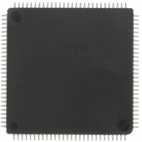
DF70845AD80FPV Renesas Electronics America, DF70845AD80FPV Datasheet - Page 950

DF70845AD80FPV
Manufacturer Part Number
DF70845AD80FPV
Description
IC SUPERH MCU FLASH 112LQFP
Manufacturer
Renesas Electronics America
Series
SuperH® SH7080r
Datasheet
1.DF70844AD80FPV.pdf
(1644 pages)
Specifications of DF70845AD80FPV
Core Size
32-Bit
Program Memory Size
512KB (512K x 8)
Core Processor
SH-2
Speed
80MHz
Connectivity
EBI/EMI, FIFO, I²C, SCI, SSU
Peripherals
DMA, POR, PWM, WDT
Number Of I /o
76
Program Memory Type
FLASH
Ram Size
32K x 8
Voltage - Supply (vcc/vdd)
3 V ~ 5.5 V
Data Converters
A/D 8x10b
Oscillator Type
Internal
Operating Temperature
-40°C ~ 85°C
Package / Case
112-LQFP
No. Of I/o's
76
Ram Memory Size
32KB
Cpu Speed
80MHz
Digital Ic Case Style
LQFP
Supply Voltage Range
3V To 3.6V, 4.5V To 5.5V
Embedded Interface Type
I2C, SCI
Rohs Compliant
Yes
Lead Free Status / RoHS Status
Lead free / RoHS Compliant
For Use With
R0K570865S001BE - KIT STARTER FOR SH7086R0K570865S000BE - KIT STARTER FOR SH7086HS0005KCU11H - EMULATOR E10A-USB H8S(X),SH2(A)
Eeprom Size
-
Lead Free Status / RoHS Status
Lead free / RoHS Compliant, Lead free / RoHS Compliant
Available stocks
Company
Part Number
Manufacturer
Quantity
Price
Company:
Part Number:
DF70845AD80FPV
Manufacturer:
TAIYO
Quantity:
40 000
Company:
Part Number:
DF70845AD80FPV
Manufacturer:
Renesas Electronics America
Quantity:
10 000
- Current page: 950 of 1644
- Download datasheet (10Mb)
Section 17 Synchronous Serial Communication Unit (SSU)
17.4.7
In clock synchronous communication mode, data communications are performed via three lines:
clock line (SSCK), data input line (SSI), and data output line (SSO).
(1)
Figure 17.12 shows an example of the initial settings in clock synchronous communication mode.
Before data transfer, clear both the TE and RE bits in SSER to 0 to set the initial values.
Note: Before changing operating modes and communications formats, clear both the TE and RE
Rev. 3.00 May 17, 2007 Page 892 of 1582
REJ09B0181-0300
[5]
Figure 17.12 Example of Initial Settings in Clock Synchronous Communication Mode
[6]
[1]
[2]
[3]
[4]
Initial Settings in Clock Synchronous Communication Mode
bits to 0. Although clearing the TE bit to 0 sets the TDRE bit to 1, clearing the RE bit to 0
does not change the values of the RDRF and ORER bits and SSRDR. Those bits retain the
previous values.
Set PFC for external pins to be used
Specify bits TE, RE, TEIE, TIE, RIE,
Clock Synchronous Communication Mode
Clear TE and RE bits in SSER to 0
Specify bits TENDSTS, SCSATS,
and CEIE in SSER simultaneously
Specify CPOS, CKS2, CKS1, and
Set SSUMS in SSCRL to 1 and
specify bits DATS1 and DATS0
(SSCK, SSI, SSO, and SCS)
Start setting initial values
and SSODTS in SSCR2
Specify MSS in SSCRH
CKS0 bits in SSMR
End
[1] Make appropriate settings in the PFC for the external
[2] Specify master/slave mode selection and SSCK pin
[3] Selects clock synchronous communication mode and
[4] Specify clock polarity selection and transfer clock rate
[5] Specify timing of TEND bit setting, SCS pin assertion, and data
[6] Enables/disables interrupt requests to the CPU.
pins to be used.
selection.
specify transmit/receive data length.
selection.
output on the SSO pin.
Related parts for DF70845AD80FPV
Image
Part Number
Description
Manufacturer
Datasheet
Request
R

Part Number:
Description:
KIT STARTER FOR M16C/29
Manufacturer:
Renesas Electronics America
Datasheet:

Part Number:
Description:
KIT STARTER FOR R8C/2D
Manufacturer:
Renesas Electronics America
Datasheet:

Part Number:
Description:
R0K33062P STARTER KIT
Manufacturer:
Renesas Electronics America
Datasheet:

Part Number:
Description:
KIT STARTER FOR R8C/23 E8A
Manufacturer:
Renesas Electronics America
Datasheet:

Part Number:
Description:
KIT STARTER FOR R8C/25
Manufacturer:
Renesas Electronics America
Datasheet:

Part Number:
Description:
KIT STARTER H8S2456 SHARPE DSPLY
Manufacturer:
Renesas Electronics America
Datasheet:

Part Number:
Description:
KIT STARTER FOR R8C38C
Manufacturer:
Renesas Electronics America
Datasheet:

Part Number:
Description:
KIT STARTER FOR R8C35C
Manufacturer:
Renesas Electronics America
Datasheet:

Part Number:
Description:
KIT STARTER FOR R8CL3AC+LCD APPS
Manufacturer:
Renesas Electronics America
Datasheet:

Part Number:
Description:
KIT STARTER FOR RX610
Manufacturer:
Renesas Electronics America
Datasheet:

Part Number:
Description:
KIT STARTER FOR R32C/118
Manufacturer:
Renesas Electronics America
Datasheet:

Part Number:
Description:
KIT DEV RSK-R8C/26-29
Manufacturer:
Renesas Electronics America
Datasheet:

Part Number:
Description:
KIT STARTER FOR SH7124
Manufacturer:
Renesas Electronics America
Datasheet:

Part Number:
Description:
KIT STARTER FOR H8SX/1622
Manufacturer:
Renesas Electronics America
Datasheet:

Part Number:
Description:
KIT DEV FOR SH7203
Manufacturer:
Renesas Electronics America
Datasheet:


