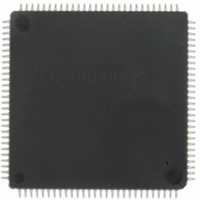
DF70845AD80FPV Renesas Electronics America, DF70845AD80FPV Datasheet - Page 887

DF70845AD80FPV
Manufacturer Part Number
DF70845AD80FPV
Description
IC SUPERH MCU FLASH 112LQFP
Manufacturer
Renesas Electronics America
Series
SuperH® SH7080r
Datasheet
1.DF70844AD80FPV.pdf
(1644 pages)
Specifications of DF70845AD80FPV
Core Size
32-Bit
Program Memory Size
512KB (512K x 8)
Core Processor
SH-2
Speed
80MHz
Connectivity
EBI/EMI, FIFO, I²C, SCI, SSU
Peripherals
DMA, POR, PWM, WDT
Number Of I /o
76
Program Memory Type
FLASH
Ram Size
32K x 8
Voltage - Supply (vcc/vdd)
3 V ~ 5.5 V
Data Converters
A/D 8x10b
Oscillator Type
Internal
Operating Temperature
-40°C ~ 85°C
Package / Case
112-LQFP
No. Of I/o's
76
Ram Memory Size
32KB
Cpu Speed
80MHz
Digital Ic Case Style
LQFP
Supply Voltage Range
3V To 3.6V, 4.5V To 5.5V
Embedded Interface Type
I2C, SCI
Rohs Compliant
Yes
Lead Free Status / RoHS Status
Lead free / RoHS Compliant
For Use With
R0K570865S001BE - KIT STARTER FOR SH7086R0K570865S000BE - KIT STARTER FOR SH7086HS0005KCU11H - EMULATOR E10A-USB H8S(X),SH2(A)
Eeprom Size
-
Lead Free Status / RoHS Status
Lead free / RoHS Compliant, Lead free / RoHS Compliant
Available stocks
Company
Part Number
Manufacturer
Quantity
Price
Company:
Part Number:
DF70845AD80FPV
Manufacturer:
TAIYO
Quantity:
40 000
Company:
Part Number:
DF70845AD80FPV
Manufacturer:
Renesas Electronics America
Quantity:
10 000
- Current page: 887 of 1644
- Download datasheet (10Mb)
16.4
16.4.1
For serial communication, the SCIF has an asynchronous mode in which characters are
synchronized individually, and a clock synchronous mode in which communication is
synchronized with clock pulses. The SCIF has a 16-byte FIFO buffer for both transmit and receive
operations, reducing the overhead of the CPU, and enabling continuous high-speed
communication. Moreover, it has RTS and CTS signals as modem control signals. The
transmission format is selected in the serial mode register (SCSMR) as shown in table 16.13. The
SCIF clock source is selected by the combination of the CKE1 and CKE0 bits in the serial control
register (SCSCR) as shown in table 16.14.
(1)
• Data length is selectable: 7 or 8 bits.
• Parity bit is selectable. So is the stop bit length (1 or 2 bits). The combination of the preceding
• In receiving, it is possible to detect framing errors, parity errors, receive FIFO data full,
• The number of stored data bytes is indicated for both the transmit and receive FIFO registers.
• An internal or external clock can be selected as the SCIF clock source.
(2)
• The transmission/reception format has a fixed 8-bit data length.
• In receiving, it is possible to detect overrun errors (ORER).
• An internal or external clock can be selected as the SCIF clock source.
selections constitutes the communication format and character length.
overrun errors, receive data ready, and breaks.
When an internal clock is selected, the SCIF operates using the on-chip baud rate
When an external clock is selected, the external clock input must have a frequency 16 times
When an internal clock is selected, the SCIF operates using the on-chip baud rate
When an external clock is selected, the SCIF operates on the input serial clock. The on-
Asynchronous Mode
Clock Synchronous Mode
generator.
the bit rate. (The on-chip baud rate generator is not used.)
generator, and outputs a serial clock signal to external devices.
chip baud rate generator is not used.
Operation
Overview
Section 16 Serial Communication Interface with FIFO (SCIF)
Rev. 3.00 May 17, 2007 Page 829 of 1582
REJ09B0181-0300
Related parts for DF70845AD80FPV
Image
Part Number
Description
Manufacturer
Datasheet
Request
R

Part Number:
Description:
KIT STARTER FOR M16C/29
Manufacturer:
Renesas Electronics America
Datasheet:

Part Number:
Description:
KIT STARTER FOR R8C/2D
Manufacturer:
Renesas Electronics America
Datasheet:

Part Number:
Description:
R0K33062P STARTER KIT
Manufacturer:
Renesas Electronics America
Datasheet:

Part Number:
Description:
KIT STARTER FOR R8C/23 E8A
Manufacturer:
Renesas Electronics America
Datasheet:

Part Number:
Description:
KIT STARTER FOR R8C/25
Manufacturer:
Renesas Electronics America
Datasheet:

Part Number:
Description:
KIT STARTER H8S2456 SHARPE DSPLY
Manufacturer:
Renesas Electronics America
Datasheet:

Part Number:
Description:
KIT STARTER FOR R8C38C
Manufacturer:
Renesas Electronics America
Datasheet:

Part Number:
Description:
KIT STARTER FOR R8C35C
Manufacturer:
Renesas Electronics America
Datasheet:

Part Number:
Description:
KIT STARTER FOR R8CL3AC+LCD APPS
Manufacturer:
Renesas Electronics America
Datasheet:

Part Number:
Description:
KIT STARTER FOR RX610
Manufacturer:
Renesas Electronics America
Datasheet:

Part Number:
Description:
KIT STARTER FOR R32C/118
Manufacturer:
Renesas Electronics America
Datasheet:

Part Number:
Description:
KIT DEV RSK-R8C/26-29
Manufacturer:
Renesas Electronics America
Datasheet:

Part Number:
Description:
KIT STARTER FOR SH7124
Manufacturer:
Renesas Electronics America
Datasheet:

Part Number:
Description:
KIT STARTER FOR H8SX/1622
Manufacturer:
Renesas Electronics America
Datasheet:

Part Number:
Description:
KIT DEV FOR SH7203
Manufacturer:
Renesas Electronics America
Datasheet:


