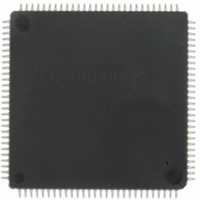
DF70845AD80FPV Renesas Electronics America, DF70845AD80FPV Datasheet - Page 892

DF70845AD80FPV
Manufacturer Part Number
DF70845AD80FPV
Description
IC SUPERH MCU FLASH 112LQFP
Manufacturer
Renesas Electronics America
Series
SuperH® SH7080r
Datasheet
1.DF70844AD80FPV.pdf
(1644 pages)
Specifications of DF70845AD80FPV
Core Size
32-Bit
Program Memory Size
512KB (512K x 8)
Core Processor
SH-2
Speed
80MHz
Connectivity
EBI/EMI, FIFO, I²C, SCI, SSU
Peripherals
DMA, POR, PWM, WDT
Number Of I /o
76
Program Memory Type
FLASH
Ram Size
32K x 8
Voltage - Supply (vcc/vdd)
3 V ~ 5.5 V
Data Converters
A/D 8x10b
Oscillator Type
Internal
Operating Temperature
-40°C ~ 85°C
Package / Case
112-LQFP
No. Of I/o's
76
Ram Memory Size
32KB
Cpu Speed
80MHz
Digital Ic Case Style
LQFP
Supply Voltage Range
3V To 3.6V, 4.5V To 5.5V
Embedded Interface Type
I2C, SCI
Rohs Compliant
Yes
Lead Free Status / RoHS Status
Lead free / RoHS Compliant
For Use With
R0K570865S001BE - KIT STARTER FOR SH7086R0K570865S000BE - KIT STARTER FOR SH7086HS0005KCU11H - EMULATOR E10A-USB H8S(X),SH2(A)
Eeprom Size
-
Lead Free Status / RoHS Status
Lead free / RoHS Compliant, Lead free / RoHS Compliant
Available stocks
Company
Part Number
Manufacturer
Quantity
Price
Company:
Part Number:
DF70845AD80FPV
Manufacturer:
TAIYO
Quantity:
40 000
Company:
Part Number:
DF70845AD80FPV
Manufacturer:
Renesas Electronics America
Quantity:
10 000
- Current page: 892 of 1644
- Download datasheet (10Mb)
Section 16 Serial Communication Interface with FIFO (SCIF)
Figure 16.3 shows a sample flowchart for initializing the SCIF.
Rev. 3.00 May 17, 2007 Page 834 of 1582
REJ09B0181-0300
and clear TFRST and RFRST bits to 0
After reading BRK, DR, and ER flags
Set PFC for external pins to be used
in SCFSR, and each flag in SCLSR,
Clear TE and RE bits in SCSCR to 0
Set TE and RE bits in SCSCR to 1,
Set data transfer format in SCSMR
(SCK, TXD, RXD, CTS, and RTS)
in SCSCR (leaving TE, RE, TIE,
and set TIE, RIE, and REIE bits
Set RTRG1-0 and TTRG1-0
Set TFRST and RFRST bits
Set CKE1 and CKE0 bits
and RIE bits cleared to 0)
and MCE bits in SCFCR,
1-bit interval elapsed?
Figure 16.3 Sample Flowchart for SCIF Initialization
write 0 to clear them
Set value in SCBRR
Start of initialization
End of initialization
in SCFCR to 1
Wait
Yes
No
[1]
[2]
[3]
[4]
[5]
[1]
[2]
[3]
[4]
[5]
Set the clock selection in SCSCR.
Be sure to clear bits TIE, RIE, TE,
and RE to 0.
Set the data transfer format in
SCSMR.
Write a value corresponding to the
bit rate into SCBRR. (Not
necessary if an external clock is
used.)
Make appropriate settings in the
PFC for the external pins to be used.
Wait at least one bit interval, then
set the TE bit or RE bit in SCSCR
to 1. Also set the RIE, REIE, and
TIE bits.
Setting the TE bit enables the TXD
and RXD pins to be used.
When transmitting, the SCIF will go
to the mark state; when receiving,
it will go to the idle state, waiting for
a start bit.
Related parts for DF70845AD80FPV
Image
Part Number
Description
Manufacturer
Datasheet
Request
R

Part Number:
Description:
KIT STARTER FOR M16C/29
Manufacturer:
Renesas Electronics America
Datasheet:

Part Number:
Description:
KIT STARTER FOR R8C/2D
Manufacturer:
Renesas Electronics America
Datasheet:

Part Number:
Description:
R0K33062P STARTER KIT
Manufacturer:
Renesas Electronics America
Datasheet:

Part Number:
Description:
KIT STARTER FOR R8C/23 E8A
Manufacturer:
Renesas Electronics America
Datasheet:

Part Number:
Description:
KIT STARTER FOR R8C/25
Manufacturer:
Renesas Electronics America
Datasheet:

Part Number:
Description:
KIT STARTER H8S2456 SHARPE DSPLY
Manufacturer:
Renesas Electronics America
Datasheet:

Part Number:
Description:
KIT STARTER FOR R8C38C
Manufacturer:
Renesas Electronics America
Datasheet:

Part Number:
Description:
KIT STARTER FOR R8C35C
Manufacturer:
Renesas Electronics America
Datasheet:

Part Number:
Description:
KIT STARTER FOR R8CL3AC+LCD APPS
Manufacturer:
Renesas Electronics America
Datasheet:

Part Number:
Description:
KIT STARTER FOR RX610
Manufacturer:
Renesas Electronics America
Datasheet:

Part Number:
Description:
KIT STARTER FOR R32C/118
Manufacturer:
Renesas Electronics America
Datasheet:

Part Number:
Description:
KIT DEV RSK-R8C/26-29
Manufacturer:
Renesas Electronics America
Datasheet:

Part Number:
Description:
KIT STARTER FOR SH7124
Manufacturer:
Renesas Electronics America
Datasheet:

Part Number:
Description:
KIT STARTER FOR H8SX/1622
Manufacturer:
Renesas Electronics America
Datasheet:

Part Number:
Description:
KIT DEV FOR SH7203
Manufacturer:
Renesas Electronics America
Datasheet:


