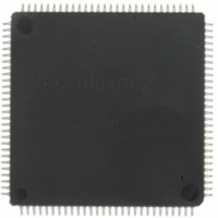
DF70845AD80FPV Renesas Electronics America, DF70845AD80FPV Datasheet - Page 415

DF70845AD80FPV
Manufacturer Part Number
DF70845AD80FPV
Description
IC SUPERH MCU FLASH 112LQFP
Manufacturer
Renesas Electronics America
Series
SuperH® SH7080r
Datasheet
1.DF70844AD80FPV.pdf
(1644 pages)
Specifications of DF70845AD80FPV
Core Size
32-Bit
Program Memory Size
512KB (512K x 8)
Core Processor
SH-2
Speed
80MHz
Connectivity
EBI/EMI, FIFO, I²C, SCI, SSU
Peripherals
DMA, POR, PWM, WDT
Number Of I /o
76
Program Memory Type
FLASH
Ram Size
32K x 8
Voltage - Supply (vcc/vdd)
3 V ~ 5.5 V
Data Converters
A/D 8x10b
Oscillator Type
Internal
Operating Temperature
-40°C ~ 85°C
Package / Case
112-LQFP
No. Of I/o's
76
Ram Memory Size
32KB
Cpu Speed
80MHz
Digital Ic Case Style
LQFP
Supply Voltage Range
3V To 3.6V, 4.5V To 5.5V
Embedded Interface Type
I2C, SCI
Rohs Compliant
Yes
Lead Free Status / RoHS Status
Lead free / RoHS Compliant
For Use With
R0K570865S001BE - KIT STARTER FOR SH7086R0K570865S000BE - KIT STARTER FOR SH7086HS0005KCU11H - EMULATOR E10A-USB H8S(X),SH2(A)
Eeprom Size
-
Lead Free Status / RoHS Status
Lead free / RoHS Compliant, Lead free / RoHS Compliant
Available stocks
Company
Part Number
Manufacturer
Quantity
Price
Company:
Part Number:
DF70845AD80FPV
Manufacturer:
TAIYO
Quantity:
40 000
Company:
Part Number:
DF70845AD80FPV
Manufacturer:
Renesas Electronics America
Quantity:
10 000
- Current page: 415 of 1644
- Download datasheet (10Mb)
9.5.12
As the operating frequency of LSIs becomes higher, the off-operation of the data buffer often
collides with the next data output when the data output from devices with slow access speed is
completed. As a result of these collisions, the reliability of the device is low and malfunctions may
occur. A function that avoids data collisions by inserting wait cycles between continuous access
cycles has been newly added.
The number of wait cycles between access cycles can be set by bits IWW[1:0], IWRWD[1:0],
IWRWS[1:0], IWRRD[1:0], and IWRRS[1:0] in CSnBCR, and bits DMAIW[1:0] and DMAIWA
in CMNCR. The conditions for setting the wait cycles between access cycles (idle cycles) are
shown below.
1. Continuous accesses are write-read or write-write
2. Continuous accesses are read-write for different spaces
3. Continuous accesses are read-write for the same space
4. Continuous accesses are read-read for different spaces
5. Continuous accesses are read-read for the same space
6. Data output cycle of an external device caused by DMA transfer in single address mode is
7. Data output cycle of an external device caused by DMA transfer in single address mode is
Besides the wait cycles between access cycles (idle cycles) described above, idle cycles must be
inserted to reserve the minimum pulse width for a multiplexed pin (WRxx), and an interface with
an internal bus.
8. Idle cycle of the external bus for the interface with the internal bus
9. Idle cycle of the external bus for accessing different memory
followed by data output from another device that includes this LSI (DMAIWA = 0)
followed by any type of access (DMAIWA = 1)
A. Insert one idle cycle immediately before a write access cycle after an external bus idle
B. Insert one idle cycle to transfer the read data to the internal bus when a read cycle of the
For accessing different memory, insert idle cycles as follows. The byte-selection SRAM
interface with the BAS bit = 1 specified is handled as an SDRAM interface because the WRxx
change timing is identical.
cycle or a read cycle.
external bus terminates.
Insert two to three idle cycles including the idle cycle in A. for the write cycle immediately
after a read cycle.
Wait between Access Cycles
Rev. 3.00 May 17, 2007 Page 357 of 1582
Section 9 Bus State Controller (BSC)
REJ09B0181-0300
Related parts for DF70845AD80FPV
Image
Part Number
Description
Manufacturer
Datasheet
Request
R

Part Number:
Description:
KIT STARTER FOR M16C/29
Manufacturer:
Renesas Electronics America
Datasheet:

Part Number:
Description:
KIT STARTER FOR R8C/2D
Manufacturer:
Renesas Electronics America
Datasheet:

Part Number:
Description:
R0K33062P STARTER KIT
Manufacturer:
Renesas Electronics America
Datasheet:

Part Number:
Description:
KIT STARTER FOR R8C/23 E8A
Manufacturer:
Renesas Electronics America
Datasheet:

Part Number:
Description:
KIT STARTER FOR R8C/25
Manufacturer:
Renesas Electronics America
Datasheet:

Part Number:
Description:
KIT STARTER H8S2456 SHARPE DSPLY
Manufacturer:
Renesas Electronics America
Datasheet:

Part Number:
Description:
KIT STARTER FOR R8C38C
Manufacturer:
Renesas Electronics America
Datasheet:

Part Number:
Description:
KIT STARTER FOR R8C35C
Manufacturer:
Renesas Electronics America
Datasheet:

Part Number:
Description:
KIT STARTER FOR R8CL3AC+LCD APPS
Manufacturer:
Renesas Electronics America
Datasheet:

Part Number:
Description:
KIT STARTER FOR RX610
Manufacturer:
Renesas Electronics America
Datasheet:

Part Number:
Description:
KIT STARTER FOR R32C/118
Manufacturer:
Renesas Electronics America
Datasheet:

Part Number:
Description:
KIT DEV RSK-R8C/26-29
Manufacturer:
Renesas Electronics America
Datasheet:

Part Number:
Description:
KIT STARTER FOR SH7124
Manufacturer:
Renesas Electronics America
Datasheet:

Part Number:
Description:
KIT STARTER FOR H8SX/1622
Manufacturer:
Renesas Electronics America
Datasheet:

Part Number:
Description:
KIT DEV FOR SH7203
Manufacturer:
Renesas Electronics America
Datasheet:


