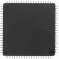
DF70845AD80FPV Renesas Electronics America, DF70845AD80FPV Datasheet - Page 1338

DF70845AD80FPV
Manufacturer Part Number
DF70845AD80FPV
Description
IC SUPERH MCU FLASH 112LQFP
Manufacturer
Renesas Electronics America
Series
SuperH® SH7080r
Datasheet
1.DF70844AD80FPV.pdf
(1644 pages)
Specifications of DF70845AD80FPV
Core Size
32-Bit
Program Memory Size
512KB (512K x 8)
Core Processor
SH-2
Speed
80MHz
Connectivity
EBI/EMI, FIFO, I²C, SCI, SSU
Peripherals
DMA, POR, PWM, WDT
Number Of I /o
76
Program Memory Type
FLASH
Ram Size
32K x 8
Voltage - Supply (vcc/vdd)
3 V ~ 5.5 V
Data Converters
A/D 8x10b
Oscillator Type
Internal
Operating Temperature
-40°C ~ 85°C
Package / Case
112-LQFP
No. Of I/o's
76
Ram Memory Size
32KB
Cpu Speed
80MHz
Digital Ic Case Style
LQFP
Supply Voltage Range
3V To 3.6V, 4.5V To 5.5V
Embedded Interface Type
I2C, SCI
Rohs Compliant
Yes
Lead Free Status / RoHS Status
Lead free / RoHS Compliant
For Use With
R0K570865S001BE - KIT STARTER FOR SH7086R0K570865S000BE - KIT STARTER FOR SH7086HS0005KCU11H - EMULATOR E10A-USB H8S(X),SH2(A)
Eeprom Size
-
Lead Free Status / RoHS Status
Lead free / RoHS Compliant, Lead free / RoHS Compliant
Available stocks
Company
Part Number
Manufacturer
Quantity
Price
Company:
Part Number:
DF70845AD80FPV
Manufacturer:
TAIYO
Quantity:
40 000
Company:
Part Number:
DF70845AD80FPV
Manufacturer:
Renesas Electronics America
Quantity:
10 000
- Current page: 1338 of 1644
- Download datasheet (10Mb)
Section 23 Flash Memory
(2) Interrupts during programming/erasing
Rev. 3.00 May 17, 2007 Page 1280 of 1582
REJ09B0181-0300
Though an interrupt processing can be executed at realtime during programming/erasing of the
downloaded on-chip program, the following limitations and notes are applied.
1. When flash memory is being programmed or erased, both the user MAT and user boot
2. Do not rewrite the program data specified by the FMPDR parameter. If new program data
3. Make sure the interrupt processing routine does not rewrite the contents of the flash-
4. At the beginning of the interrupt processing routine, save the CPU register contents. Before
5. When a transition is made to sleep mode or software standby mode in the interrupt
MAT cannot be accessed. Prepare the interrupt vector table and interrupt processing
routine in on-chip RAM or external memory. Make sure the flash memory being
programmed or erased is not accessed by the interrupt processing routine. If flash memory
is read, the read values are not guaranteed. If the relevant bank in flash memory that is
being programmed or erased is accessed, the error protection state is entered, and
programming or erasing is aborted. If a bank other than the relevant bank is accessed, the
error protection state is not entered but the read values are not guaranteed.
is to provided by the interrupt processing, temporarily save the new program data in
another area. After confirming the completion of programming, save the new program data
in the area specified by FMPDR or change the setting in FMPDR to indicated the other
area in which the new program data was temporarily saved.
memory related registers or data in the downloaded on-chip program area. During the
interrupt processing, do not simultaneously perform RAM emulation, download of the on-
chip program by an SCO request, or programming/erasing.
returning from the interrupt processing, write the saved contents in the CPU registers again.
processing routine, the error protection state is entered and programming/erasing is
aborted.
If a transition is made to the reset state, the reset signal should only be released after
providing a reset input over a period longer than the normal 100 µs to reduce the damage to
flash memory.
Related parts for DF70845AD80FPV
Image
Part Number
Description
Manufacturer
Datasheet
Request
R

Part Number:
Description:
KIT STARTER FOR M16C/29
Manufacturer:
Renesas Electronics America
Datasheet:

Part Number:
Description:
KIT STARTER FOR R8C/2D
Manufacturer:
Renesas Electronics America
Datasheet:

Part Number:
Description:
R0K33062P STARTER KIT
Manufacturer:
Renesas Electronics America
Datasheet:

Part Number:
Description:
KIT STARTER FOR R8C/23 E8A
Manufacturer:
Renesas Electronics America
Datasheet:

Part Number:
Description:
KIT STARTER FOR R8C/25
Manufacturer:
Renesas Electronics America
Datasheet:

Part Number:
Description:
KIT STARTER H8S2456 SHARPE DSPLY
Manufacturer:
Renesas Electronics America
Datasheet:

Part Number:
Description:
KIT STARTER FOR R8C38C
Manufacturer:
Renesas Electronics America
Datasheet:

Part Number:
Description:
KIT STARTER FOR R8C35C
Manufacturer:
Renesas Electronics America
Datasheet:

Part Number:
Description:
KIT STARTER FOR R8CL3AC+LCD APPS
Manufacturer:
Renesas Electronics America
Datasheet:

Part Number:
Description:
KIT STARTER FOR RX610
Manufacturer:
Renesas Electronics America
Datasheet:

Part Number:
Description:
KIT STARTER FOR R32C/118
Manufacturer:
Renesas Electronics America
Datasheet:

Part Number:
Description:
KIT DEV RSK-R8C/26-29
Manufacturer:
Renesas Electronics America
Datasheet:

Part Number:
Description:
KIT STARTER FOR SH7124
Manufacturer:
Renesas Electronics America
Datasheet:

Part Number:
Description:
KIT STARTER FOR H8SX/1622
Manufacturer:
Renesas Electronics America
Datasheet:

Part Number:
Description:
KIT DEV FOR SH7203
Manufacturer:
Renesas Electronics America
Datasheet:


