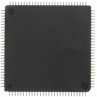
DF70845AD80FPV Renesas Electronics America, DF70845AD80FPV Datasheet - Page 359

DF70845AD80FPV
Manufacturer Part Number
DF70845AD80FPV
Description
IC SUPERH MCU FLASH 112LQFP
Manufacturer
Renesas Electronics America
Series
SuperH® SH7080r
Datasheet
1.DF70844AD80FPV.pdf
(1644 pages)
Specifications of DF70845AD80FPV
Core Size
32-Bit
Program Memory Size
512KB (512K x 8)
Core Processor
SH-2
Speed
80MHz
Connectivity
EBI/EMI, FIFO, I²C, SCI, SSU
Peripherals
DMA, POR, PWM, WDT
Number Of I /o
76
Program Memory Type
FLASH
Ram Size
32K x 8
Voltage - Supply (vcc/vdd)
3 V ~ 5.5 V
Data Converters
A/D 8x10b
Oscillator Type
Internal
Operating Temperature
-40°C ~ 85°C
Package / Case
112-LQFP
No. Of I/o's
76
Ram Memory Size
32KB
Cpu Speed
80MHz
Digital Ic Case Style
LQFP
Supply Voltage Range
3V To 3.6V, 4.5V To 5.5V
Embedded Interface Type
I2C, SCI
Rohs Compliant
Yes
Lead Free Status / RoHS Status
Lead free / RoHS Compliant
For Use With
R0K570865S001BE - KIT STARTER FOR SH7086R0K570865S000BE - KIT STARTER FOR SH7086HS0005KCU11H - EMULATOR E10A-USB H8S(X),SH2(A)
Eeprom Size
-
Lead Free Status / RoHS Status
Lead free / RoHS Compliant, Lead free / RoHS Compliant
Available stocks
Company
Part Number
Manufacturer
Quantity
Price
Company:
Part Number:
DF70845AD80FPV
Manufacturer:
TAIYO
Quantity:
40 000
Company:
Part Number:
DF70845AD80FPV
Manufacturer:
Renesas Electronics America
Quantity:
10 000
- Current page: 359 of 1644
- Download datasheet (10Mb)
Section 9 Bus State Controller (BSC)
9.5.6
SDRAM Interface
SDRAM Direct Connection: The SDRAM that can be connected to this LSI is a product that has
11/12/13 bits of row address, 8/9/10 bits of column address, 4 or less banks, and uses the A10 pin
for setting precharge mode in read and write command cycles.
The control signals for direct connection of SDRAM are RASU, RASL, CASU, CASL, RDWR,
DQMUU, DQMLU, DQMLL, CKE, CS2, and CS3. All the signals other than CS2 and CS3 are
common to all areas, and signals other than CKE are valid when CS2 or CS3 is asserted. SDRAM
can be connected to up to 2 spaces. The data bus width of the area that is connected to SDRAM
can be set to 32 or 16 bits.
Burst read/single write (burst length 1) and burst read/burst write (burst length 1) are supported as
SDRAM operating mode.
Commands for SDRAM can be specified by RASU, RASL, CASU, CASL, RDWR, and specific
address signals. These commands are shown below.
• NOP
• Auto-refresh (REF)
• Self-refresh (SELF)
• All banks precharge (PALL)
• Specified bank precharge (PRE)
• Bank active (ACTV)
• Read (READ)
• Read with precharge (READA)
• Write (WRIT)
• Write with precharge (WRITA)
• Write mode register (MRS)
The byte to be accessed is specified by DQMUU, DQMUL, DQMLU and DQMLL. Reading or
writing is performed for a byte whose corresponding DQMxx low. For details on the relationship
between DQMxx and the byte to be accessed, refer to section 9.5.1, Endian/Access Size and Data
Alignment.
Figures 9.14 to 9.16 show shows an example of the connection of SDRAM with the LSI.
Rev. 3.00 May 17, 2007 Page 301 of 1582
REJ09B0181-0300
Related parts for DF70845AD80FPV
Image
Part Number
Description
Manufacturer
Datasheet
Request
R

Part Number:
Description:
KIT STARTER FOR M16C/29
Manufacturer:
Renesas Electronics America
Datasheet:

Part Number:
Description:
KIT STARTER FOR R8C/2D
Manufacturer:
Renesas Electronics America
Datasheet:

Part Number:
Description:
R0K33062P STARTER KIT
Manufacturer:
Renesas Electronics America
Datasheet:

Part Number:
Description:
KIT STARTER FOR R8C/23 E8A
Manufacturer:
Renesas Electronics America
Datasheet:

Part Number:
Description:
KIT STARTER FOR R8C/25
Manufacturer:
Renesas Electronics America
Datasheet:

Part Number:
Description:
KIT STARTER H8S2456 SHARPE DSPLY
Manufacturer:
Renesas Electronics America
Datasheet:

Part Number:
Description:
KIT STARTER FOR R8C38C
Manufacturer:
Renesas Electronics America
Datasheet:

Part Number:
Description:
KIT STARTER FOR R8C35C
Manufacturer:
Renesas Electronics America
Datasheet:

Part Number:
Description:
KIT STARTER FOR R8CL3AC+LCD APPS
Manufacturer:
Renesas Electronics America
Datasheet:

Part Number:
Description:
KIT STARTER FOR RX610
Manufacturer:
Renesas Electronics America
Datasheet:

Part Number:
Description:
KIT STARTER FOR R32C/118
Manufacturer:
Renesas Electronics America
Datasheet:

Part Number:
Description:
KIT DEV RSK-R8C/26-29
Manufacturer:
Renesas Electronics America
Datasheet:

Part Number:
Description:
KIT STARTER FOR SH7124
Manufacturer:
Renesas Electronics America
Datasheet:

Part Number:
Description:
KIT STARTER FOR H8SX/1622
Manufacturer:
Renesas Electronics America
Datasheet:

Part Number:
Description:
KIT DEV FOR SH7203
Manufacturer:
Renesas Electronics America
Datasheet:


