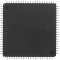
DF70845AD80FPV Renesas Electronics America, DF70845AD80FPV Datasheet - Page 38

DF70845AD80FPV
Manufacturer Part Number
DF70845AD80FPV
Description
IC SUPERH MCU FLASH 112LQFP
Manufacturer
Renesas Electronics America
Series
SuperH® SH7080r
Datasheet
1.DF70844AD80FPV.pdf
(1644 pages)
Specifications of DF70845AD80FPV
Core Size
32-Bit
Program Memory Size
512KB (512K x 8)
Core Processor
SH-2
Speed
80MHz
Connectivity
EBI/EMI, FIFO, I²C, SCI, SSU
Peripherals
DMA, POR, PWM, WDT
Number Of I /o
76
Program Memory Type
FLASH
Ram Size
32K x 8
Voltage - Supply (vcc/vdd)
3 V ~ 5.5 V
Data Converters
A/D 8x10b
Oscillator Type
Internal
Operating Temperature
-40°C ~ 85°C
Package / Case
112-LQFP
No. Of I/o's
76
Ram Memory Size
32KB
Cpu Speed
80MHz
Digital Ic Case Style
LQFP
Supply Voltage Range
3V To 3.6V, 4.5V To 5.5V
Embedded Interface Type
I2C, SCI
Rohs Compliant
Yes
Lead Free Status / RoHS Status
Lead free / RoHS Compliant
For Use With
R0K570865S001BE - KIT STARTER FOR SH7086R0K570865S000BE - KIT STARTER FOR SH7086HS0005KCU11H - EMULATOR E10A-USB H8S(X),SH2(A)
Eeprom Size
-
Lead Free Status / RoHS Status
Lead free / RoHS Compliant, Lead free / RoHS Compliant
Available stocks
Company
Part Number
Manufacturer
Quantity
Price
Company:
Part Number:
DF70845AD80FPV
Manufacturer:
TAIYO
Quantity:
40 000
Company:
Part Number:
DF70845AD80FPV
Manufacturer:
Renesas Electronics America
Quantity:
10 000
- Current page: 38 of 1644
- Download datasheet (10Mb)
Figure 13.3 Low-Level Detection Operation.............................................................................. 708
Figure 13.4 Output-Level Compare Operation........................................................................... 708
Figure 13.5 Pin State when a Power-On Reset is Issued from the Watchdog Timer.................. 711
Section 14 Watchdog Timer (WDT)
Figure 14.1 Block Diagram of WDT .......................................................................................... 714
Figure 14.2 Writing to WTCNT and WTCSR............................................................................ 719
Figure 14.3 Operation in Watchdog Timer Mode
Section 15 Serial Communication Interface (SCI)
Figure 15.1 Block Diagram of SCI............................................................................................. 724
Figure 15.2 Example of Data Format in Asynchronous Communication
Figure 15.3 Sample Flowchart for SCI Initialization.................................................................. 759
Figure 15.4 Sample Flowchart for Transmitting Serial Data...................................................... 760
Figure 15.5 Example of Transmission in Asynchronous Mode
Figure 15.6 Sample Flowchart for Receiving Serial Data (1)..................................................... 763
Figure 15.6 Sample Flowchart for Receiving Serial Data (2)..................................................... 764
Figure 15.7 Example of SCI Receive Operation (8-Bit Data, Parity, One Stop Bit) .................. 766
Figure 15.8 Data Format in Clock Synchronous Communication.............................................. 766
Figure 15.9 Sample Flowchart for SCI Initialization.................................................................. 768
Figure 15.10 Sample Flowchart for Transmitting Serial Data.................................................... 769
Figure 15.11 Example of SCI Transmit Operation..................................................................... 770
Figure 15.12 Sample Flowchart for Receiving Serial Data (1)................................................... 771
Figure 15.12 Sample Flowchart for Receiving Serial Data (2)................................................... 772
Figure 15.13 Example of SCI Receive Operation ...................................................................... 773
Figure 15.14 Sample Flowchart for Transmitting/Receiving Serial Data................................... 774
Figure 15.15 Example of Communication Using Multiprocessor Format
Figure 15.16 Sample Multiprocessor Serial Transmission Flowchart ........................................ 777
Figure 15.17 Example of SCI Operation in Reception
Figure 15.18 Sample Multiprocessor Serial Reception Flowchart (1)........................................ 779
Figure 15.18 Sample Multiprocessor Serial Reception Flowchart (2)........................................ 780
Figure 15.19 SCKIO Bit, SCKDT bit, and SCK Pin .................................................................. 782
Figure 15.20 SPBIO Bit, SPBDT bit, and TXD Pin................................................................... 783
Figure 15.21 Receive Data Sampling Timing in Asynchronous Mode ...................................... 786
Figure 15.22 Example of Clock Synchronous Transfer Using DMAC or DTC ......................... 787
Rev. 3.00 May 17, 2007 Page xxxviii of Iviii
(When WTCNT Count Clock is Specified to Pφ/32 by CKS2 to CKS0) ................ 721
(8-Bit Data with Parity and Two Stop Bits) ............................................................ 756
(8-Bit Data, Parity, One Stop Bit) ........................................................................... 762
(Transmission of Data H'AA to Receiving Station A) .......................................... 776
(Example with 8-Bit Data, Multiprocessor Bit, One Stop Bit).............................. 778
Related parts for DF70845AD80FPV
Image
Part Number
Description
Manufacturer
Datasheet
Request
R

Part Number:
Description:
KIT STARTER FOR M16C/29
Manufacturer:
Renesas Electronics America
Datasheet:

Part Number:
Description:
KIT STARTER FOR R8C/2D
Manufacturer:
Renesas Electronics America
Datasheet:

Part Number:
Description:
R0K33062P STARTER KIT
Manufacturer:
Renesas Electronics America
Datasheet:

Part Number:
Description:
KIT STARTER FOR R8C/23 E8A
Manufacturer:
Renesas Electronics America
Datasheet:

Part Number:
Description:
KIT STARTER FOR R8C/25
Manufacturer:
Renesas Electronics America
Datasheet:

Part Number:
Description:
KIT STARTER H8S2456 SHARPE DSPLY
Manufacturer:
Renesas Electronics America
Datasheet:

Part Number:
Description:
KIT STARTER FOR R8C38C
Manufacturer:
Renesas Electronics America
Datasheet:

Part Number:
Description:
KIT STARTER FOR R8C35C
Manufacturer:
Renesas Electronics America
Datasheet:

Part Number:
Description:
KIT STARTER FOR R8CL3AC+LCD APPS
Manufacturer:
Renesas Electronics America
Datasheet:

Part Number:
Description:
KIT STARTER FOR RX610
Manufacturer:
Renesas Electronics America
Datasheet:

Part Number:
Description:
KIT STARTER FOR R32C/118
Manufacturer:
Renesas Electronics America
Datasheet:

Part Number:
Description:
KIT DEV RSK-R8C/26-29
Manufacturer:
Renesas Electronics America
Datasheet:

Part Number:
Description:
KIT STARTER FOR SH7124
Manufacturer:
Renesas Electronics America
Datasheet:

Part Number:
Description:
KIT STARTER FOR H8SX/1622
Manufacturer:
Renesas Electronics America
Datasheet:

Part Number:
Description:
KIT DEV FOR SH7203
Manufacturer:
Renesas Electronics America
Datasheet:


