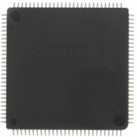
DF70845AD80FPV Renesas Electronics America, DF70845AD80FPV Datasheet - Page 1607

DF70845AD80FPV
Manufacturer Part Number
DF70845AD80FPV
Description
IC SUPERH MCU FLASH 112LQFP
Manufacturer
Renesas Electronics America
Series
SuperH® SH7080r
Datasheet
1.DF70844AD80FPV.pdf
(1644 pages)
Specifications of DF70845AD80FPV
Core Size
32-Bit
Program Memory Size
512KB (512K x 8)
Core Processor
SH-2
Speed
80MHz
Connectivity
EBI/EMI, FIFO, I²C, SCI, SSU
Peripherals
DMA, POR, PWM, WDT
Number Of I /o
76
Program Memory Type
FLASH
Ram Size
32K x 8
Voltage - Supply (vcc/vdd)
3 V ~ 5.5 V
Data Converters
A/D 8x10b
Oscillator Type
Internal
Operating Temperature
-40°C ~ 85°C
Package / Case
112-LQFP
No. Of I/o's
76
Ram Memory Size
32KB
Cpu Speed
80MHz
Digital Ic Case Style
LQFP
Supply Voltage Range
3V To 3.6V, 4.5V To 5.5V
Embedded Interface Type
I2C, SCI
Rohs Compliant
Yes
Lead Free Status / RoHS Status
Lead free / RoHS Compliant
For Use With
R0K570865S001BE - KIT STARTER FOR SH7086R0K570865S000BE - KIT STARTER FOR SH7086HS0005KCU11H - EMULATOR E10A-USB H8S(X),SH2(A)
Eeprom Size
-
Lead Free Status / RoHS Status
Lead free / RoHS Compliant, Lead free / RoHS Compliant
Available stocks
Company
Part Number
Manufacturer
Quantity
Price
Company:
Part Number:
DF70845AD80FPV
Manufacturer:
TAIYO
Quantity:
40 000
Company:
Part Number:
DF70845AD80FPV
Manufacturer:
Renesas Electronics America
Quantity:
10 000
- Current page: 1607 of 1644
- Download datasheet (10Mb)
Item
9.5.14 Others
9.5.15 Access to On-Chip FLASH
and On-Chip RAM by CPU to
9.5.17 Access to External Memory
by CPU
Table 10.6 Selecting On-Chip
Peripheral Module Request
Modes with RS3 to RS0 Bits
10.4.6 Operation Timing
Table 10.9 Number of Cycles per
Access to On-Chip RAM by
DMAC
Page Revision (See Manual for Details)
377
378
to
382
401
419,
420
423
Deleted
(2) Access in View of LSI Internal Bus Master
…….
(3) On-Chip Peripheral Module Access
Added
Amended
Notes: ADDR4 to ADDR7: A/D data register in A/D
Added
Note added.
Notes: 2. The number of cycles for access to the on-
RS3 RS2 RS1 RS0
1
0
converter channel 1
chip peripheral I/O or an external device are
indicated in section 9.5.16, Access to On-Chip
Peripheral I/O Registers by CPU, and section
9.5.17, Access to External Memory by CPU.
The access cycles are obtained by subtracting
the cycles of Iφ required for L-bus access from
the cycles required for access by the CPU.
1
1
Rev. 3.00 May 17, 2007 Page 1549 of 1582
Transfer
Request
Source
A/D_1
Transfer
Request
Signal
ADI1
REJ09B0181-0300
Source
ADDR4 to ADDR7
Related parts for DF70845AD80FPV
Image
Part Number
Description
Manufacturer
Datasheet
Request
R

Part Number:
Description:
KIT STARTER FOR M16C/29
Manufacturer:
Renesas Electronics America
Datasheet:

Part Number:
Description:
KIT STARTER FOR R8C/2D
Manufacturer:
Renesas Electronics America
Datasheet:

Part Number:
Description:
R0K33062P STARTER KIT
Manufacturer:
Renesas Electronics America
Datasheet:

Part Number:
Description:
KIT STARTER FOR R8C/23 E8A
Manufacturer:
Renesas Electronics America
Datasheet:

Part Number:
Description:
KIT STARTER FOR R8C/25
Manufacturer:
Renesas Electronics America
Datasheet:

Part Number:
Description:
KIT STARTER H8S2456 SHARPE DSPLY
Manufacturer:
Renesas Electronics America
Datasheet:

Part Number:
Description:
KIT STARTER FOR R8C38C
Manufacturer:
Renesas Electronics America
Datasheet:

Part Number:
Description:
KIT STARTER FOR R8C35C
Manufacturer:
Renesas Electronics America
Datasheet:

Part Number:
Description:
KIT STARTER FOR R8CL3AC+LCD APPS
Manufacturer:
Renesas Electronics America
Datasheet:

Part Number:
Description:
KIT STARTER FOR RX610
Manufacturer:
Renesas Electronics America
Datasheet:

Part Number:
Description:
KIT STARTER FOR R32C/118
Manufacturer:
Renesas Electronics America
Datasheet:

Part Number:
Description:
KIT DEV RSK-R8C/26-29
Manufacturer:
Renesas Electronics America
Datasheet:

Part Number:
Description:
KIT STARTER FOR SH7124
Manufacturer:
Renesas Electronics America
Datasheet:

Part Number:
Description:
KIT STARTER FOR H8SX/1622
Manufacturer:
Renesas Electronics America
Datasheet:

Part Number:
Description:
KIT DEV FOR SH7203
Manufacturer:
Renesas Electronics America
Datasheet:


