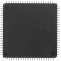
DF70845AD80FPV Renesas Electronics America, DF70845AD80FPV Datasheet - Page 146

DF70845AD80FPV
Manufacturer Part Number
DF70845AD80FPV
Description
IC SUPERH MCU FLASH 112LQFP
Manufacturer
Renesas Electronics America
Series
SuperH® SH7080r
Datasheet
1.DF70844AD80FPV.pdf
(1644 pages)
Specifications of DF70845AD80FPV
Core Size
32-Bit
Program Memory Size
512KB (512K x 8)
Core Processor
SH-2
Speed
80MHz
Connectivity
EBI/EMI, FIFO, I²C, SCI, SSU
Peripherals
DMA, POR, PWM, WDT
Number Of I /o
76
Program Memory Type
FLASH
Ram Size
32K x 8
Voltage - Supply (vcc/vdd)
3 V ~ 5.5 V
Data Converters
A/D 8x10b
Oscillator Type
Internal
Operating Temperature
-40°C ~ 85°C
Package / Case
112-LQFP
No. Of I/o's
76
Ram Memory Size
32KB
Cpu Speed
80MHz
Digital Ic Case Style
LQFP
Supply Voltage Range
3V To 3.6V, 4.5V To 5.5V
Embedded Interface Type
I2C, SCI
Rohs Compliant
Yes
Lead Free Status / RoHS Status
Lead free / RoHS Compliant
For Use With
R0K570865S001BE - KIT STARTER FOR SH7086R0K570865S000BE - KIT STARTER FOR SH7086HS0005KCU11H - EMULATOR E10A-USB H8S(X),SH2(A)
Eeprom Size
-
Lead Free Status / RoHS Status
Lead free / RoHS Compliant, Lead free / RoHS Compliant
Available stocks
Company
Part Number
Manufacturer
Quantity
Price
Company:
Part Number:
DF70845AD80FPV
Manufacturer:
TAIYO
Quantity:
40 000
Company:
Part Number:
DF70845AD80FPV
Manufacturer:
Renesas Electronics America
Quantity:
10 000
- Current page: 146 of 1644
- Download datasheet (10Mb)
Section 5 Exception Handling
5.1.2
The exceptions are detected and the exception handling starts according to the timing shown in
table 5.2.
Table 5.2
When exception handling starts, the CPU operates
Exception Handling Triggered by Reset: The initial values of the program counter (PC) and
stack pointer (SP) are fetched from the exception handling vector table (PC from the address
H'00000000 and SP from the address H'00000004 when a power-on reset. PC from the address
H'00000008 and SP from the address H'0000000C when a manual reset.). For details, see section
5.1.3, Exception Handling Vector Table. H'00000000 is then written to the vector base register
(VBR), and H'F (B'1111) is written to the interrupt mask bits (I3 to I0) in the status register (SR).
The program starts from the PC address fetched from the exception handling vector table.
Exception Handling Triggered by Address Error, Interrupt, and Instruction: SR and PC are
saved to the stack indicated by R15. For interrupt exception handling, the interrupt priority level is
written to the interrupt mask bits (I3 to I0) in SR. For address error and instruction exception
handling, bits I3 to I0 are not affected. The start address is then fetched from the exception
handling vector table and the program starts from that address.
Rev. 3.00 May 17, 2007 Page 88 of 1582
REJ09B0181-0300
Exception
Reset
Address error
Interrupt
Instruction
Exception Handling Operations
Timing for Exception Detection and Start of Exception Handling
Power-on reset
Manual reset
Trap instruction
General illegal
instructions
Illegal slot
instructions
Timing of Source Detection and Start of Exception Handling
Started when the RES pin changes from low to high or when the
WDT overflows.
Started when the MRES pin changes from low to high or when the
WDT overflows.
Detected during the instruction decode stage and started after the
execution of the current instruction is completed.
Started by the execution of the TRAPA instruction.
Started when an undefined code placed at other than a delay slot
(immediately after a delayed branch instruction) is decoded.
Started when an undefined code placed at a delay slot
(immediately after a delayed branch instruction) or an instruction
that changes the PC value is detected.
Related parts for DF70845AD80FPV
Image
Part Number
Description
Manufacturer
Datasheet
Request
R

Part Number:
Description:
KIT STARTER FOR M16C/29
Manufacturer:
Renesas Electronics America
Datasheet:

Part Number:
Description:
KIT STARTER FOR R8C/2D
Manufacturer:
Renesas Electronics America
Datasheet:

Part Number:
Description:
R0K33062P STARTER KIT
Manufacturer:
Renesas Electronics America
Datasheet:

Part Number:
Description:
KIT STARTER FOR R8C/23 E8A
Manufacturer:
Renesas Electronics America
Datasheet:

Part Number:
Description:
KIT STARTER FOR R8C/25
Manufacturer:
Renesas Electronics America
Datasheet:

Part Number:
Description:
KIT STARTER H8S2456 SHARPE DSPLY
Manufacturer:
Renesas Electronics America
Datasheet:

Part Number:
Description:
KIT STARTER FOR R8C38C
Manufacturer:
Renesas Electronics America
Datasheet:

Part Number:
Description:
KIT STARTER FOR R8C35C
Manufacturer:
Renesas Electronics America
Datasheet:

Part Number:
Description:
KIT STARTER FOR R8CL3AC+LCD APPS
Manufacturer:
Renesas Electronics America
Datasheet:

Part Number:
Description:
KIT STARTER FOR RX610
Manufacturer:
Renesas Electronics America
Datasheet:

Part Number:
Description:
KIT STARTER FOR R32C/118
Manufacturer:
Renesas Electronics America
Datasheet:

Part Number:
Description:
KIT DEV RSK-R8C/26-29
Manufacturer:
Renesas Electronics America
Datasheet:

Part Number:
Description:
KIT STARTER FOR SH7124
Manufacturer:
Renesas Electronics America
Datasheet:

Part Number:
Description:
KIT STARTER FOR H8SX/1622
Manufacturer:
Renesas Electronics America
Datasheet:

Part Number:
Description:
KIT DEV FOR SH7203
Manufacturer:
Renesas Electronics America
Datasheet:


