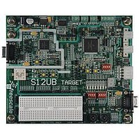
LFEBS12UB Freescale Semiconductor, LFEBS12UB Datasheet - Page 72

LFEBS12UB
Manufacturer Part Number
LFEBS12UB
Description
KIT STUDENT LEARNING S12 DG128
Manufacturer
Freescale Semiconductor
Specifications of LFEBS12UB
Architecture
8/16-bit
Code Gen Tools Included
Code Warrior
Silicon Manufacturer
Freescale
Core Architecture
S12
Core Sub-architecture
S12
Silicon Core Number
MC9S12
Silicon Family Name
S12D
Kit Contents
HCS12 DG128 Learning Kit
Rohs Compliant
Yes
Lead Free Status / RoHS Status
Lead free / RoHS Compliant
- Current page: 72 of 1328
- Download datasheet (9Mb)
Chapter 1 Device Overview MC9S12XE-Family
1.2.3.76
PS0 is a general-purpose input or output pin. It can be configured as the receive pin RXD of serial
communication interface 0 (SCI0).
1.2.3.77
PT[7:6] are general-purpose input or output pins. They can be configured as input capture or output
compare pins IOC[7:6] of the enhanced capture timer (ECT).
1.2.3.78
PT[5] is a general-purpose input or output pin. It can be configured as input capture or output compare pin
IOC[5] of the enhanced capture timer (ECT) or can be configured to output the VREG_API signal.
1.2.3.79
PT[4:0] are general-purpose input or output pins. They can be configured as input capture or output
compare pins IOC[4:0] of the enhanced capture timer (ECT).
1.2.4
MC9S12XE-Family power and ground pins are described below.
Because fast signal transitions place high, short-duration current demands on the power supply, use bypass
capacitors with high-frequency characteristics and place them as close to the MCU as possible.
1.2.4.1
External power and ground for I/O drivers. Bypass requirements depend on how heavily the MCU pins are
loaded. All V
1.2.4.2
Input to the internal voltage regulator. The internal voltage regulator is turned off, if V
1.2.4.3
Power is supplied to the MCU core from the internal voltage regulator, whose load capacitor must be
connected to VDD. The voltage supply of nominally 1.8V is derived from the internal voltage regulator.
The return current path is through the VSS1,VSS2 and VSS3 pins. No static external loading of these pins
is permitted.
72
Because of an order from the United States International Trade Commission, BGA-packaged product lines and partnumbers
indicated here currently are not available from Freescale for import or sale in the United States prior to September 2010
Power Supply Pins
PS0 / RXD0 — Port S I/O Pin 0
PT[7:6] / IOC[7:6] — Port T I/O Pins [7:6]
PT[5] / IOC[5] / VREG_API— Port T I/O Pins [5]
PT[4:0] / IOC[4:0] — Port T I/O Pins [4:0]
VDDX[7:1], VSSX[7:1] — Power and Ground Pins for I/O Drivers
DDX
VDDR — Power Pin for Internal Voltage Regulator
VDD, VSS1,VSS2,VSS3 — Core Power Pins
All V
pins are connected together internally. All V
SS
pins must be connected together in the application.
MC9S12XE-Family Reference Manual , Rev. 1.23
NOTE
SSX
pins are connected together internally.
Freescale Semiconductor
DDR
is tied to ground
Related parts for LFEBS12UB
Image
Part Number
Description
Manufacturer
Datasheet
Request
R
Part Number:
Description:
Manufacturer:
Freescale Semiconductor, Inc
Datasheet:
Part Number:
Description:
Manufacturer:
Freescale Semiconductor, Inc
Datasheet:
Part Number:
Description:
Manufacturer:
Freescale Semiconductor, Inc
Datasheet:
Part Number:
Description:
Manufacturer:
Freescale Semiconductor, Inc
Datasheet:
Part Number:
Description:
Manufacturer:
Freescale Semiconductor, Inc
Datasheet:
Part Number:
Description:
Manufacturer:
Freescale Semiconductor, Inc
Datasheet:
Part Number:
Description:
Manufacturer:
Freescale Semiconductor, Inc
Datasheet:
Part Number:
Description:
Manufacturer:
Freescale Semiconductor, Inc
Datasheet:
Part Number:
Description:
Manufacturer:
Freescale Semiconductor, Inc
Datasheet:
Part Number:
Description:
Manufacturer:
Freescale Semiconductor, Inc
Datasheet:
Part Number:
Description:
Manufacturer:
Freescale Semiconductor, Inc
Datasheet:
Part Number:
Description:
Manufacturer:
Freescale Semiconductor, Inc
Datasheet:
Part Number:
Description:
Manufacturer:
Freescale Semiconductor, Inc
Datasheet:
Part Number:
Description:
Manufacturer:
Freescale Semiconductor, Inc
Datasheet:
Part Number:
Description:
Manufacturer:
Freescale Semiconductor, Inc
Datasheet:


