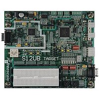
LFEBS12UB Freescale Semiconductor, LFEBS12UB Datasheet - Page 508

LFEBS12UB
Manufacturer Part Number
LFEBS12UB
Description
KIT STUDENT LEARNING S12 DG128
Manufacturer
Freescale Semiconductor
Specifications of LFEBS12UB
Architecture
8/16-bit
Code Gen Tools Included
Code Warrior
Silicon Manufacturer
Freescale
Core Architecture
S12
Core Sub-architecture
S12
Silicon Core Number
MC9S12
Silicon Family Name
S12D
Kit Contents
HCS12 DG128 Learning Kit
Rohs Compliant
Yes
Lead Free Status / RoHS Status
Lead free / RoHS Compliant
- Current page: 508 of 1328
- Download datasheet (9Mb)
Chapter 13 Analog-to-Digital Converter (ADC12B16CV1)
13.2
This section lists all inputs to the ADC12B16C block.
13.2.1
13.2.1.1
This pin serves as the analog input Channel x. It can also be configured as digital port or external trigger
for the ATD conversion.
13.2.1.2
These inputs can be configured to serve as an external trigger for the ATD conversion.
Refer to device specification for availability and connection of these inputs!
13.2.1.3
V
13.2.1.4
These pins are the power supplies for the analog circuitry of the ADC12B16C block.
13.3
This section provides a detailed description of all registers accessible in the ADC12B16C.
13.3.1
Figure 13-2
508
Address
0x0000
0x0001
0x0002
Because of an order from the United States International Trade Commission, BGA-packaged product lines and partnumbers
RH
indicated here currently are not available from Freescale for import or sale in the United States prior to September 2010
is the high reference voltage, V
Signal Description
Memory Map and Register Definition
ATDCTL0
ATDCTL1
ATDCTL2
Detailed Signal Descriptions
Module Memory Map
Name
gives an overview on all ADC12B16C registers.
ANx (x = 15, 14, 13, 12, 11, 10, 9, 8, 7, 6, 5, 4, 3, 2, 1, 0)
ETRIG3, ETRIG2, ETRIG1, ETRIG0
V
V
Register Address = Base Address + Address Offset, where the Base Address
is defined at the MCU level and the Address Offset is defined at the module
level.
RH
DDA
, V
, V
W
W
W
RL
R
R
R
SSA
Figure 13-2. ADC12B16C Register Summary (Sheet 1 of 3)
ETRIGSEL
Reserved
Bit 7
0
MC9S12XE-Family Reference Manual , Rev. 1.23
= Unimplemented or Reserved
SRES1
RL
AFFC
6
0
is the low reference voltage for ATD conversion.
ICLKSTP ETRIGLE
SRES0
5
0
NOTE
SMP_DIS ETRIGCH3 ETRIGCH2 ETRIGCH1 ETRIGCH0
4
0
ETRIGP
WRAP3
3
ETRIGE
WRAP2
2
Freescale Semiconductor
WRAP1
ASCIE
1
ACMPIE
WRAP0
Bit 0
Related parts for LFEBS12UB
Image
Part Number
Description
Manufacturer
Datasheet
Request
R
Part Number:
Description:
Manufacturer:
Freescale Semiconductor, Inc
Datasheet:
Part Number:
Description:
Manufacturer:
Freescale Semiconductor, Inc
Datasheet:
Part Number:
Description:
Manufacturer:
Freescale Semiconductor, Inc
Datasheet:
Part Number:
Description:
Manufacturer:
Freescale Semiconductor, Inc
Datasheet:
Part Number:
Description:
Manufacturer:
Freescale Semiconductor, Inc
Datasheet:
Part Number:
Description:
Manufacturer:
Freescale Semiconductor, Inc
Datasheet:
Part Number:
Description:
Manufacturer:
Freescale Semiconductor, Inc
Datasheet:
Part Number:
Description:
Manufacturer:
Freescale Semiconductor, Inc
Datasheet:
Part Number:
Description:
Manufacturer:
Freescale Semiconductor, Inc
Datasheet:
Part Number:
Description:
Manufacturer:
Freescale Semiconductor, Inc
Datasheet:
Part Number:
Description:
Manufacturer:
Freescale Semiconductor, Inc
Datasheet:
Part Number:
Description:
Manufacturer:
Freescale Semiconductor, Inc
Datasheet:
Part Number:
Description:
Manufacturer:
Freescale Semiconductor, Inc
Datasheet:
Part Number:
Description:
Manufacturer:
Freescale Semiconductor, Inc
Datasheet:
Part Number:
Description:
Manufacturer:
Freescale Semiconductor, Inc
Datasheet:


