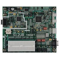
LFEBS12UB Freescale Semiconductor, LFEBS12UB Datasheet - Page 1238

LFEBS12UB
Manufacturer Part Number
LFEBS12UB
Description
KIT STUDENT LEARNING S12 DG128
Manufacturer
Freescale Semiconductor
Specifications of LFEBS12UB
Architecture
8/16-bit
Code Gen Tools Included
Code Warrior
Silicon Manufacturer
Freescale
Core Architecture
S12
Core Sub-architecture
S12
Silicon Core Number
MC9S12
Silicon Family Name
S12D
Kit Contents
HCS12 DG128 Learning Kit
Rohs Compliant
Yes
Lead Free Status / RoHS Status
Lead free / RoHS Compliant
- Current page: 1238 of 1328
- Download datasheet (9Mb)
Appendix A Electrical Characteristics
A.6.1.2
Provided an appropriate external reset signal is applied to the MCU, preventing the CPU from executing
code when V
the PORF bit in the CRG flags register has not been set.
A.6.1.3
When external reset is asserted for a time greater than PW
reset, and the CPU starts fetching the reset vector without doing a clock quality check, if there was an
oscillation before reset.
A.6.1.4
Out of stop the controller can be woken up by an external interrupt. A clock quality check as after POR is
performed before releasing the clocks to the system.
If the MCU is woken-up by an interrupt and the fast wake-up feature is enabled (FSTWKP = 1 and
SCME = 1), the system will resume operation in self-clock mode after t
A.6.1.5
The recovery from pseudo stop and wait is essentially the same since the oscillator is not stopped in both
modes. The controller can be woken up by internal or external interrupts. After t
the interrupt vector.
1238
DD35
SRAM Data Retention
External Reset
Stop Recovery
Pseudo Stop and Wait Recovery
is out of specification limits, the SRAM contents integrity is guaranteed if after the reset
MC9S12XE-Family Reference Manual , Rev. 1.23
RSTL
the CRG module generates an internal
fws
.
wrs
the CPU starts fetching
Freescale Semiconductor
Related parts for LFEBS12UB
Image
Part Number
Description
Manufacturer
Datasheet
Request
R
Part Number:
Description:
Manufacturer:
Freescale Semiconductor, Inc
Datasheet:
Part Number:
Description:
Manufacturer:
Freescale Semiconductor, Inc
Datasheet:
Part Number:
Description:
Manufacturer:
Freescale Semiconductor, Inc
Datasheet:
Part Number:
Description:
Manufacturer:
Freescale Semiconductor, Inc
Datasheet:
Part Number:
Description:
Manufacturer:
Freescale Semiconductor, Inc
Datasheet:
Part Number:
Description:
Manufacturer:
Freescale Semiconductor, Inc
Datasheet:
Part Number:
Description:
Manufacturer:
Freescale Semiconductor, Inc
Datasheet:
Part Number:
Description:
Manufacturer:
Freescale Semiconductor, Inc
Datasheet:
Part Number:
Description:
Manufacturer:
Freescale Semiconductor, Inc
Datasheet:
Part Number:
Description:
Manufacturer:
Freescale Semiconductor, Inc
Datasheet:
Part Number:
Description:
Manufacturer:
Freescale Semiconductor, Inc
Datasheet:
Part Number:
Description:
Manufacturer:
Freescale Semiconductor, Inc
Datasheet:
Part Number:
Description:
Manufacturer:
Freescale Semiconductor, Inc
Datasheet:
Part Number:
Description:
Manufacturer:
Freescale Semiconductor, Inc
Datasheet:
Part Number:
Description:
Manufacturer:
Freescale Semiconductor, Inc
Datasheet:


