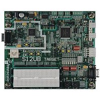
LFEBS12UB Freescale Semiconductor, LFEBS12UB Datasheet - Page 190

LFEBS12UB
Manufacturer Part Number
LFEBS12UB
Description
KIT STUDENT LEARNING S12 DG128
Manufacturer
Freescale Semiconductor
Specifications of LFEBS12UB
Architecture
8/16-bit
Code Gen Tools Included
Code Warrior
Silicon Manufacturer
Freescale
Core Architecture
S12
Core Sub-architecture
S12
Silicon Core Number
MC9S12
Silicon Family Name
S12D
Kit Contents
HCS12 DG128 Learning Kit
Rohs Compliant
Yes
Lead Free Status / RoHS Status
Lead free / RoHS Compliant
- Current page: 190 of 1328
- Download datasheet (9Mb)
Chapter 2 Port Integration Module (S12XEPIMV1)
t
pulse
Figure 2-109. Pulse Illustration
A valid edge on an input is detected if 4 consecutive samples of a passive level are followed by 4
consecutive samples of an active level directly or indirectly.
The filters are continuously clocked by the bus clock in RUN and WAIT mode. In STOP mode the clock
is generated by an RC-oscillator in the Port Integration Module. To maximize current saving the RC
oscillator runs only if the following condition is true on any pin individually:
Sample count <= 4 and interrupt enabled (PIE=1) and interrupt flag not set (PIF=0)
2.5
Initialization Information
2.5.1
Port Data and Data Direction Register writes
It is not recommended to write PORTx/PTx and DDRx in a word access. When changing the register pins
from inputs to outputs, the data may have extra transitions during the write access. Initialize the port data
register before enabling the outputs.
MC9S12XE-Family Reference Manual , Rev. 1.23
190
Freescale Semiconductor
Related parts for LFEBS12UB
Image
Part Number
Description
Manufacturer
Datasheet
Request
R
Part Number:
Description:
Manufacturer:
Freescale Semiconductor, Inc
Datasheet:
Part Number:
Description:
Manufacturer:
Freescale Semiconductor, Inc
Datasheet:
Part Number:
Description:
Manufacturer:
Freescale Semiconductor, Inc
Datasheet:
Part Number:
Description:
Manufacturer:
Freescale Semiconductor, Inc
Datasheet:
Part Number:
Description:
Manufacturer:
Freescale Semiconductor, Inc
Datasheet:
Part Number:
Description:
Manufacturer:
Freescale Semiconductor, Inc
Datasheet:
Part Number:
Description:
Manufacturer:
Freescale Semiconductor, Inc
Datasheet:
Part Number:
Description:
Manufacturer:
Freescale Semiconductor, Inc
Datasheet:
Part Number:
Description:
Manufacturer:
Freescale Semiconductor, Inc
Datasheet:
Part Number:
Description:
Manufacturer:
Freescale Semiconductor, Inc
Datasheet:
Part Number:
Description:
Manufacturer:
Freescale Semiconductor, Inc
Datasheet:
Part Number:
Description:
Manufacturer:
Freescale Semiconductor, Inc
Datasheet:
Part Number:
Description:
Manufacturer:
Freescale Semiconductor, Inc
Datasheet:
Part Number:
Description:
Manufacturer:
Freescale Semiconductor, Inc
Datasheet:
Part Number:
Description:
Manufacturer:
Freescale Semiconductor, Inc
Datasheet:


