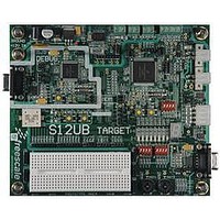
LFEBS12UB Freescale Semiconductor, LFEBS12UB Datasheet - Page 388

LFEBS12UB
Manufacturer Part Number
LFEBS12UB
Description
KIT STUDENT LEARNING S12 DG128
Manufacturer
Freescale Semiconductor
Specifications of LFEBS12UB
Architecture
8/16-bit
Code Gen Tools Included
Code Warrior
Silicon Manufacturer
Freescale
Core Architecture
S12
Core Sub-architecture
S12
Silicon Core Number
MC9S12
Silicon Family Name
S12D
Kit Contents
HCS12 DG128 Learning Kit
Rohs Compliant
Yes
Lead Free Status / RoHS Status
Lead free / RoHS Compliant
- Current page: 388 of 1328
- Download datasheet (9Mb)
Chapter 10 XGATE (S12XGATEV3)
10.8.2.2
All logic and arithmetic instructions support the 8 bit immediate addressing mode (IMM8: RD = RD ∗
#IMM8) and the triadic addressing mode (TRI: RD = RS1 ∗ RS2).
All arithmetic is considered as signed, sign, overflow, zero and carry flag will be updated. The carry will
not be affected for logical operations.
10.8.2.3
This group comprises transfers from and to some special registers
Branch Instructions
The branch offset is +255 words or -256 words counted from the beginning of the next instruction. Since
instructions have a fixed 16 bit width, the branch offsets are word aligned by shifting the offset value by 2.
An unconditional branch allows a +511 words or -512 words branch distance.
10.8.2.4
Shift operations allow the use of a 4 bit wide immediate value to identify a shift width within a 16 bit word.
For shift operations a value of 0 does not shift at all, while a value of 15 shifts the register RD by 15 bits.
In a second form the shift value is contained in the bits 3:0 of the register RS.
Examples:
388
Because of an order from the United States International Trade Commission, BGA-packaged product lines and partnumbers
indicated here currently are not available from Freescale for import or sale in the United States prior to September 2010
ADDL
ANDH
ADD
SUB
AND
OR
TFR
BEQ
BRA
LSL
LSR
ASR
Logic and Arithmetic Instructions
Register – Register Transfers
Shift Instructions
R2,#1
R4,#$FE
R3,R4,R5
R3,R4,R5
R3,R4,R5
R3,R4,R5
R3,CCR
label
label
R4,#1
R4,#3
R4,R2
; R4 = R4 << 1; shift register R4 by 1 bit to the left
; R4 = R4 >> 3; shift register R4 by 3 bits to the right
; R4 = R4 >> R2;arithmetic shift register R4 right by the amount
;
MC9S12XE-Family Reference Manual , Rev. 1.23
; increment R2
; R4.H = R4.H & $FE, clear lower bit of higher byte
; R3 = R4 + R5
; R3 = R4 - R5
; R3 = R4 & R5 logical AND on the whole word
; R3 = R4 | R5
; transfers the condition code register to the low byte of
; register R3
; if Z flag = 1 branch to label
of bits contained in R2[3:0].
Freescale Semiconductor
Related parts for LFEBS12UB
Image
Part Number
Description
Manufacturer
Datasheet
Request
R
Part Number:
Description:
Manufacturer:
Freescale Semiconductor, Inc
Datasheet:
Part Number:
Description:
Manufacturer:
Freescale Semiconductor, Inc
Datasheet:
Part Number:
Description:
Manufacturer:
Freescale Semiconductor, Inc
Datasheet:
Part Number:
Description:
Manufacturer:
Freescale Semiconductor, Inc
Datasheet:
Part Number:
Description:
Manufacturer:
Freescale Semiconductor, Inc
Datasheet:
Part Number:
Description:
Manufacturer:
Freescale Semiconductor, Inc
Datasheet:
Part Number:
Description:
Manufacturer:
Freescale Semiconductor, Inc
Datasheet:
Part Number:
Description:
Manufacturer:
Freescale Semiconductor, Inc
Datasheet:
Part Number:
Description:
Manufacturer:
Freescale Semiconductor, Inc
Datasheet:
Part Number:
Description:
Manufacturer:
Freescale Semiconductor, Inc
Datasheet:
Part Number:
Description:
Manufacturer:
Freescale Semiconductor, Inc
Datasheet:
Part Number:
Description:
Manufacturer:
Freescale Semiconductor, Inc
Datasheet:
Part Number:
Description:
Manufacturer:
Freescale Semiconductor, Inc
Datasheet:
Part Number:
Description:
Manufacturer:
Freescale Semiconductor, Inc
Datasheet:
Part Number:
Description:
Manufacturer:
Freescale Semiconductor, Inc
Datasheet:


