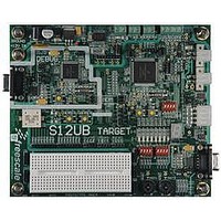
LFEBS12UB Freescale Semiconductor, LFEBS12UB Datasheet - Page 289

LFEBS12UB
Manufacturer Part Number
LFEBS12UB
Description
KIT STUDENT LEARNING S12 DG128
Manufacturer
Freescale Semiconductor
Specifications of LFEBS12UB
Architecture
8/16-bit
Code Gen Tools Included
Code Warrior
Silicon Manufacturer
Freescale
Core Architecture
S12
Core Sub-architecture
S12
Silicon Core Number
MC9S12
Silicon Family Name
S12D
Kit Contents
HCS12 DG128 Learning Kit
Rohs Compliant
Yes
Lead Free Status / RoHS Status
Lead free / RoHS Compliant
- Current page: 289 of 1328
- Download datasheet (9Mb)
7.3.2.4
Register Global Address 0x7FFF08
Read: All modes through BDM operation when not secured
Write: All modes through BDM operation when not secured
7.3.3
The family ID is a 8-bit value located in the firmware ROM (at global address: 0x7FFF0F). The read-only
value is a unique family ID which is 0xC1 for S12X devices.
7.4
The BDM receives and executes commands from a host via a single wire serial interface. There are two
types of BDM commands: hardware and firmware commands.
Hardware commands are used to read and write target system memory locations and to enter active
background debug mode, see
includes all memory that is accessible by the CPU.
Firmware commands are used to read and write CPU resources and to exit from active background debug
mode, see
accumulator (D), X index register (X), Y index register (Y), stack pointer (SP), and program counter (PC).
Hardware commands can be executed at any time and in any mode excluding a few exceptions as
highlighted (see
“Security”). Firmware commands can only be executed when the system is not secure and is in active
background debug mode (BDM).
Freescale Semiconductor
Because of an order from the United States International Trade Commission, BGA-packaged product lines and partnumbers
BGP[6:0]
Reset
indicated here currently are not available from Freescale for import or sale in the United States prior to September 2010
BGAE
Field
6–0
7
W
R
Functional Description
Section 7.4.4, “Standard BDM Firmware
BGAE
Family ID Assignment
BDM Global Page Access Enable Bit — BGAE enables global page access for BDM hardware and firmware
read/write instructions The BDM hardware commands used to access the BDM registers (READ_BD_ and
WRITE_BD_) can not be used for global accesses even if the BGAE bit is set.
0 BDM Global Access disabled
1 BDM Global Access enabled
BDM Global Page Index Bits 6–0 — These bits define the extended address bits from 22 to 16. For more
detailed information regarding the global page window scheme, please refer to the S12X_MMC Block Guide.
BDM Global Page Index Register (BDMGPR)
7
0
Section 7.4.3, “BDM Hardware
BGP6
6
0
Figure 7-6. BDM Global Page Register (BDMGPR)
Section 7.4.3, “BDM Hardware
MC9S12XE-Family Reference Manual Rev. 1.23
Table 7-5. BDMGPR Field Descriptions
BGP5
5
0
BGP4
Commands”) and in secure mode (see
4
0
Commands”. The CPU resources referred to are the
Description
BGP3
Commands”. Target system memory
3
0
Chapter 7 Background Debug Module (S12XBDMV2)
BGP2
2
0
BGP1
1
0
Section 7.4.1,
BGP0
0
0
289
Related parts for LFEBS12UB
Image
Part Number
Description
Manufacturer
Datasheet
Request
R
Part Number:
Description:
Manufacturer:
Freescale Semiconductor, Inc
Datasheet:
Part Number:
Description:
Manufacturer:
Freescale Semiconductor, Inc
Datasheet:
Part Number:
Description:
Manufacturer:
Freescale Semiconductor, Inc
Datasheet:
Part Number:
Description:
Manufacturer:
Freescale Semiconductor, Inc
Datasheet:
Part Number:
Description:
Manufacturer:
Freescale Semiconductor, Inc
Datasheet:
Part Number:
Description:
Manufacturer:
Freescale Semiconductor, Inc
Datasheet:
Part Number:
Description:
Manufacturer:
Freescale Semiconductor, Inc
Datasheet:
Part Number:
Description:
Manufacturer:
Freescale Semiconductor, Inc
Datasheet:
Part Number:
Description:
Manufacturer:
Freescale Semiconductor, Inc
Datasheet:
Part Number:
Description:
Manufacturer:
Freescale Semiconductor, Inc
Datasheet:
Part Number:
Description:
Manufacturer:
Freescale Semiconductor, Inc
Datasheet:
Part Number:
Description:
Manufacturer:
Freescale Semiconductor, Inc
Datasheet:
Part Number:
Description:
Manufacturer:
Freescale Semiconductor, Inc
Datasheet:
Part Number:
Description:
Manufacturer:
Freescale Semiconductor, Inc
Datasheet:
Part Number:
Description:
Manufacturer:
Freescale Semiconductor, Inc
Datasheet:


