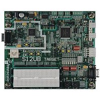
LFEBS12UB Freescale Semiconductor, LFEBS12UB Datasheet - Page 253

LFEBS12UB
Manufacturer Part Number
LFEBS12UB
Description
KIT STUDENT LEARNING S12 DG128
Manufacturer
Freescale Semiconductor
Specifications of LFEBS12UB
Architecture
8/16-bit
Code Gen Tools Included
Code Warrior
Silicon Manufacturer
Freescale
Core Architecture
S12
Core Sub-architecture
S12
Silicon Core Number
MC9S12
Silicon Family Name
S12D
Kit Contents
HCS12 DG128 Learning Kit
Rohs Compliant
Yes
Lead Free Status / RoHS Status
Lead free / RoHS Compliant
- Current page: 253 of 1328
- Download datasheet (9Mb)
1. Incl. S12X_EBI registers
2. Refer to S12X_MMC section.
3. If EWAIT enabled for at least one CSx line (refer to S12X_MMC section), the minimum number of external bus cycles is 3.
4. Available only if configured appropriately by ROMON and EROMON (refer to S12X_MMC section).
5.4.2
Internal visibility allows the observation of the internal CPU address and data bus as well as the
determination of the access source and the CPU pipe (queue) status through the external bus interface.
Internal visibility is always enabled in emulation single chip mode and emulation expanded mode. Internal
CPU accesses are made visible on the external bus interface except CPU execution of BDM firmware
instructions.
Internal reads are made visible on ADDRx/IVDx (address and read data multiplexed, see
Table
show the type of access. External read data are also visible on IVDx.
During ‘no access’ cycles RW is held in read position while LSTRB is undetermined.
All accesses which make use of the external bus interface are considered external accesses.
Freescale Semiconductor
Data direction signals
threshold enabled on
Because of an order from the United States International Trade Commission, BGA-packaged product lines and partnumbers
Data select signals
(if 16-bit data bus)
address access
indicated here currently are not available from Freescale for import or sale in the United States prior to September 2010
Reduced input
External wait
Chip Selects
(if Enabled)
Bus signals
Properties
Flash area
5-14), internal writes on ADDRx and DATAx (see
feature
Internal Visibility
(4)
Single-Chip
Normal
Single-Chip Modes
—
—
—
—
—
—
—
Table 5-9. Summary of Functions (continued)
MC9S12XE-Family Reference Manual Rev. 1.23
Single-Chip
Special
—
—
—
—
—
—
—
Signal Properties
ADDR[22:1]
Expanded
DATA[15:0]
Table 5-4
Normal
Refer to
EWAIT
UDS
LDS
CS0
CS1
CS2
CS3
WE
RE
—
Table 5-15
ADDR[22:20]/
ADDR[19:16]/
Single-Chip
ADDR[15:0]/
IQSTAT[3:0]
DATA[15:0]
DATA[15:0]
Emulation
IVD[15:0]
ACC[2:0]
ADDR0
1 cycle
LSTRB
EWAIT
RW
Chapter 5 External Bus Interface (S12XEBIV4)
—
—
Expanded Modes
to
Table
ADDR[22:20]/
ADDR[19:16]/
5-17). RW and LSTRB
ADDR[15:0]/
IQSTAT[3:0]
DATA[15:0]
DATA[15:0]
Emulation
Expanded
IVD[15:0]
ACC[2:0]
ADDR0
LSTRB
1 cycle
EWAIT
EWAIT
CS0
CS1
CS2
CS3
RW
Table 5-12
ADDR[22:0]
DATA[15:0]
Table 5-4
Special
Refer to
ADDR0
LSTRB
1 cycle
Test
RW
—
—
to
253
Related parts for LFEBS12UB
Image
Part Number
Description
Manufacturer
Datasheet
Request
R
Part Number:
Description:
Manufacturer:
Freescale Semiconductor, Inc
Datasheet:
Part Number:
Description:
Manufacturer:
Freescale Semiconductor, Inc
Datasheet:
Part Number:
Description:
Manufacturer:
Freescale Semiconductor, Inc
Datasheet:
Part Number:
Description:
Manufacturer:
Freescale Semiconductor, Inc
Datasheet:
Part Number:
Description:
Manufacturer:
Freescale Semiconductor, Inc
Datasheet:
Part Number:
Description:
Manufacturer:
Freescale Semiconductor, Inc
Datasheet:
Part Number:
Description:
Manufacturer:
Freescale Semiconductor, Inc
Datasheet:
Part Number:
Description:
Manufacturer:
Freescale Semiconductor, Inc
Datasheet:
Part Number:
Description:
Manufacturer:
Freescale Semiconductor, Inc
Datasheet:
Part Number:
Description:
Manufacturer:
Freescale Semiconductor, Inc
Datasheet:
Part Number:
Description:
Manufacturer:
Freescale Semiconductor, Inc
Datasheet:
Part Number:
Description:
Manufacturer:
Freescale Semiconductor, Inc
Datasheet:
Part Number:
Description:
Manufacturer:
Freescale Semiconductor, Inc
Datasheet:
Part Number:
Description:
Manufacturer:
Freescale Semiconductor, Inc
Datasheet:
Part Number:
Description:
Manufacturer:
Freescale Semiconductor, Inc
Datasheet:


