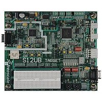
LFEBS12UB Freescale Semiconductor, LFEBS12UB Datasheet - Page 259

LFEBS12UB
Manufacturer Part Number
LFEBS12UB
Description
KIT STUDENT LEARNING S12 DG128
Manufacturer
Freescale Semiconductor
Specifications of LFEBS12UB
Architecture
8/16-bit
Code Gen Tools Included
Code Warrior
Silicon Manufacturer
Freescale
Core Architecture
S12
Core Sub-architecture
S12
Silicon Core Number
MC9S12
Silicon Family Name
S12D
Kit Contents
HCS12 DG128 Learning Kit
Rohs Compliant
Yes
Lead Free Status / RoHS Status
Lead free / RoHS Compliant
- Current page: 259 of 1328
- Download datasheet (9Mb)
internal RAM and misaligned XGATE PRR accesses in emulation modes are the only type of access that
are able to produce LSTRB = ADDR0 = 1. This is summarized in
Freescale Semiconductor
Word write of data on DATA[15:0] at an even and even+1
address
Byte write of data on DATA[7:0] at an odd address
Byte write of data on DATA[15:8] at an even address
Word write at an odd and odd+1 internal RAM address
(misaligned — only in emulation modes)
Word read of data on DATA[15:0] at an even and even+1
address
Byte read of data on DATA[7:0] at an odd address
Byte read of data on DATA[15:8] at an even address
Word read at an odd and odd+1 internal RAM address
(misaligned - only in emulation modes)
Because of an order from the United States International Trade Commission, BGA-packaged product lines and partnumbers
indicated here currently are not available from Freescale for import or sale in the United States prior to September 2010
Table 5-20. Access in Emulation Modes and Special Test Mode
Access
MC9S12XE-Family Reference Manual Rev. 1.23
RW LSTRB ADDR0
0
0
0
0
1
1
1
1
0
0
1
1
0
0
1
1
Table
0
1
0
1
0
1
0
1
Chapter 5 External Bus Interface (S12XEBIV4)
Out
Out
Out data(odd+1) Out
I/O
5-20.
In
In
In
In
In
DATA[15:8]
data(odd+1)
data(addr)
data(even)
data(even)
data(even)
data(odd)
x
x
Out
Out
I/O
In
In
In
In
In
DATA[7:0]
data(even+1)
data(addr)
data(odd)
data(odd)
data(odd)
data(odd)
data(odd)
x
x
259
Related parts for LFEBS12UB
Image
Part Number
Description
Manufacturer
Datasheet
Request
R
Part Number:
Description:
Manufacturer:
Freescale Semiconductor, Inc
Datasheet:
Part Number:
Description:
Manufacturer:
Freescale Semiconductor, Inc
Datasheet:
Part Number:
Description:
Manufacturer:
Freescale Semiconductor, Inc
Datasheet:
Part Number:
Description:
Manufacturer:
Freescale Semiconductor, Inc
Datasheet:
Part Number:
Description:
Manufacturer:
Freescale Semiconductor, Inc
Datasheet:
Part Number:
Description:
Manufacturer:
Freescale Semiconductor, Inc
Datasheet:
Part Number:
Description:
Manufacturer:
Freescale Semiconductor, Inc
Datasheet:
Part Number:
Description:
Manufacturer:
Freescale Semiconductor, Inc
Datasheet:
Part Number:
Description:
Manufacturer:
Freescale Semiconductor, Inc
Datasheet:
Part Number:
Description:
Manufacturer:
Freescale Semiconductor, Inc
Datasheet:
Part Number:
Description:
Manufacturer:
Freescale Semiconductor, Inc
Datasheet:
Part Number:
Description:
Manufacturer:
Freescale Semiconductor, Inc
Datasheet:
Part Number:
Description:
Manufacturer:
Freescale Semiconductor, Inc
Datasheet:
Part Number:
Description:
Manufacturer:
Freescale Semiconductor, Inc
Datasheet:
Part Number:
Description:
Manufacturer:
Freescale Semiconductor, Inc
Datasheet:


