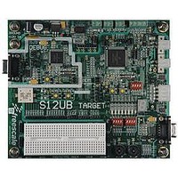
LFEBS12UB Freescale Semiconductor, LFEBS12UB Datasheet - Page 63

LFEBS12UB
Manufacturer Part Number
LFEBS12UB
Description
KIT STUDENT LEARNING S12 DG128
Manufacturer
Freescale Semiconductor
Specifications of LFEBS12UB
Architecture
8/16-bit
Code Gen Tools Included
Code Warrior
Silicon Manufacturer
Freescale
Core Architecture
S12
Core Sub-architecture
S12
Silicon Core Number
MC9S12
Silicon Family Name
S12D
Kit Contents
HCS12 DG128 Learning Kit
Rohs Compliant
Yes
Lead Free Status / RoHS Status
Lead free / RoHS Compliant
- Current page: 63 of 1328
- Download datasheet (9Mb)
1.2.3.7
PA[7:0] are general-purpose input or output pins. In MCU expanded modes of operation, these pins are
used for the external address bus. In MCU emulation modes of operation, these pins are used for external
address bus and internal visibility read data.
1.2.3.8
PB[7:1] are general-purpose input or output pins. In MCU expanded modes of operation, these pins are
used for the external address bus. In MCU emulation modes of operation, these pins are used for external
address bus and internal visibility read data.
1.2.3.9
PB0 is a general-purpose input or output pin. In MCU expanded modes of operation, this pin is used for
the external address bus ADDR0 or as upper data strobe signal. In MCU emulation modes of operation,
this pin is used for external address bus ADDR0 and internal visibility read data IVD0.
1.2.3.10
PC[7:0] are general-purpose input or output pins. In MCU expanded modes of operation, these pins are
used for the external data bus.
The input voltage thresholds for PC[7:0] can be configured to reduced levels, to allow data from an external
3.3-V peripheral to be read by the MCU operating at 5.0 V. The input voltage thresholds for PC[7:0] are
configured to reduced levels out of reset in expanded and emulation modes. The input voltage thresholds
for PC[7:0] are configured to 5-V levels out of reset in normal modes.
1.2.3.11
PD[7:0] are general-purpose input or output pins. In MCU expanded modes of operation, these pins are
used for the external data bus.
The input voltage thresholds for PD[7:0] can be configured to reduced levels, to allow data from an
external 3.3-V peripheral to be read by the MCU operating at 5.0 V. The input voltage thresholds for
PD[7:0] are configured to reduced levels out of reset in expanded and emulation modes. The input voltage
thresholds for PC[7:0] are configured to 5-V levels out of reset in normal modes.
1.2.3.12
PE7 is a general-purpose input or output pin. ECLKX2 is a free running clock of twice the internal bus
frequency, available by default in emulation modes and when enabled in other modes. The XCLKS is an
input signal which controls whether a crystal in combination with the internal loop controlled Pierce
oscillator is used or whether full swing Pierce oscillator/external clock circuitry is used (refer to
Configuration). An internal pullup is enabled during reset.
Freescale Semiconductor
Because of an order from the United States International Trade Commission, BGA-packaged product lines and partnumbers
indicated here currently are not available from Freescale for import or sale in the United States prior to September 2010
PA[7:0] / ADDR[15:8] / IVD[15:8] — Port A I/O Pins
PB[7:1] / ADDR[7:1] / IVD[7:1] — Port B I/O Pins
PB0 / ADDR0 / UDS / IVD[0] — Port B I/O Pin 0
PC[7:0] / DATA [15:8] — Port C I/O Pins
PD[7:0] / DATA [7:0] — Port D I/O Pins
PE7 / ECLKX2 / XCLKS — Port E I/O Pin 7
MC9S12XE-Family Reference Manual Rev. 1.23
Chapter 1 Device Overview MC9S12XE-Family
Oscillator
63
Related parts for LFEBS12UB
Image
Part Number
Description
Manufacturer
Datasheet
Request
R
Part Number:
Description:
Manufacturer:
Freescale Semiconductor, Inc
Datasheet:
Part Number:
Description:
Manufacturer:
Freescale Semiconductor, Inc
Datasheet:
Part Number:
Description:
Manufacturer:
Freescale Semiconductor, Inc
Datasheet:
Part Number:
Description:
Manufacturer:
Freescale Semiconductor, Inc
Datasheet:
Part Number:
Description:
Manufacturer:
Freescale Semiconductor, Inc
Datasheet:
Part Number:
Description:
Manufacturer:
Freescale Semiconductor, Inc
Datasheet:
Part Number:
Description:
Manufacturer:
Freescale Semiconductor, Inc
Datasheet:
Part Number:
Description:
Manufacturer:
Freescale Semiconductor, Inc
Datasheet:
Part Number:
Description:
Manufacturer:
Freescale Semiconductor, Inc
Datasheet:
Part Number:
Description:
Manufacturer:
Freescale Semiconductor, Inc
Datasheet:
Part Number:
Description:
Manufacturer:
Freescale Semiconductor, Inc
Datasheet:
Part Number:
Description:
Manufacturer:
Freescale Semiconductor, Inc
Datasheet:
Part Number:
Description:
Manufacturer:
Freescale Semiconductor, Inc
Datasheet:
Part Number:
Description:
Manufacturer:
Freescale Semiconductor, Inc
Datasheet:
Part Number:
Description:
Manufacturer:
Freescale Semiconductor, Inc
Datasheet:


