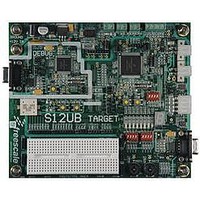
LFEBS12UB Freescale Semiconductor, LFEBS12UB Datasheet - Page 652

LFEBS12UB
Manufacturer Part Number
LFEBS12UB
Description
KIT STUDENT LEARNING S12 DG128
Manufacturer
Freescale Semiconductor
Specifications of LFEBS12UB
Architecture
8/16-bit
Code Gen Tools Included
Code Warrior
Silicon Manufacturer
Freescale
Core Architecture
S12
Core Sub-architecture
S12
Silicon Core Number
MC9S12
Silicon Family Name
S12D
Kit Contents
HCS12 DG128 Learning Kit
Rohs Compliant
Yes
Lead Free Status / RoHS Status
Lead free / RoHS Compliant
- Current page: 652 of 1328
- Download datasheet (9Mb)
Chapter 16 Freescale’s Scalable Controller Area Network (S12MSCANV3)
The synchronization jump width (see the Bosch CAN 2.0A/B specification for details) can be programmed
in a range of 1 to 4 time quanta by setting the SJW parameter.
The SYNC_SEG, TSEG1, TSEG2, and SJW parameters are set by programming the MSCAN bus timing
registers (CANBTR0, CANBTR1) (see
and
Table 16-37
related parameter values.
16.4.4
16.4.4.1
The MSCAN module behaves as described within this specification in all normal system operating modes.
Write restrictions exist for some registers.
652
Section 16.3.2.4, “MSCAN Bus Timing Register 1
Time Segment 1
Modes of Operation
gives an overview of the Bosch CAN 2.0A/B specification compliant segment settings and the
Normal System Operating Modes
5 .. 10
4 .. 11
5 .. 12
6 .. 13
7 .. 14
8 .. 15
9 .. 16
It is the user’s responsibility to ensure the bit time settings are in compliance
with the CAN standard.
Transmit Point
Sample Point
Table 16-37. Bosch CAN 2.0A/B Compliant Bit Time Segment Settings
SYNC_SEG
Syntax
TSEG1
3 .. 10
4 .. 11
5 .. 12
6 .. 13
7 .. 14
8 .. 15
4 .. 9
MC9S12XE-Family Reference Manual , Rev. 1.23
System expects transitions to occur on the CAN bus during this
period.
A node in transmit mode transfers a new value to the CAN bus at
this point.
A node in receive mode samples the CAN bus at this point. If the
three samples per bit option is selected, then this point marks the
position of the third sample.
Table 16-36. Time Segment Syntax
Time Segment 2
Section 16.3.2.3, “MSCAN Bus Timing Register 0
2
3
4
5
6
7
8
NOTE
(CANBTR1)”).
Description
TSEG2
1
2
3
4
5
6
7
Synchronization
Jump Width
1 .. 2
1 .. 3
1 .. 4
1 .. 4
1 .. 4
1 .. 4
1 .. 4
Freescale Semiconductor
(CANBTR0)”
SJW
0 .. 1
0 .. 2
0 .. 3
0 .. 3
0 .. 3
0 .. 3
0 .. 3
Related parts for LFEBS12UB
Image
Part Number
Description
Manufacturer
Datasheet
Request
R
Part Number:
Description:
Manufacturer:
Freescale Semiconductor, Inc
Datasheet:
Part Number:
Description:
Manufacturer:
Freescale Semiconductor, Inc
Datasheet:
Part Number:
Description:
Manufacturer:
Freescale Semiconductor, Inc
Datasheet:
Part Number:
Description:
Manufacturer:
Freescale Semiconductor, Inc
Datasheet:
Part Number:
Description:
Manufacturer:
Freescale Semiconductor, Inc
Datasheet:
Part Number:
Description:
Manufacturer:
Freescale Semiconductor, Inc
Datasheet:
Part Number:
Description:
Manufacturer:
Freescale Semiconductor, Inc
Datasheet:
Part Number:
Description:
Manufacturer:
Freescale Semiconductor, Inc
Datasheet:
Part Number:
Description:
Manufacturer:
Freescale Semiconductor, Inc
Datasheet:
Part Number:
Description:
Manufacturer:
Freescale Semiconductor, Inc
Datasheet:
Part Number:
Description:
Manufacturer:
Freescale Semiconductor, Inc
Datasheet:
Part Number:
Description:
Manufacturer:
Freescale Semiconductor, Inc
Datasheet:
Part Number:
Description:
Manufacturer:
Freescale Semiconductor, Inc
Datasheet:
Part Number:
Description:
Manufacturer:
Freescale Semiconductor, Inc
Datasheet:
Part Number:
Description:
Manufacturer:
Freescale Semiconductor, Inc
Datasheet:


