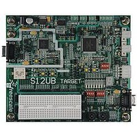
LFEBS12UB Freescale Semiconductor, LFEBS12UB Datasheet - Page 1216

LFEBS12UB
Manufacturer Part Number
LFEBS12UB
Description
KIT STUDENT LEARNING S12 DG128
Manufacturer
Freescale Semiconductor
Specifications of LFEBS12UB
Architecture
8/16-bit
Code Gen Tools Included
Code Warrior
Silicon Manufacturer
Freescale
Core Architecture
S12
Core Sub-architecture
S12
Silicon Core Number
MC9S12
Silicon Family Name
S12D
Kit Contents
HCS12 DG128 Learning Kit
Rohs Compliant
Yes
Lead Free Status / RoHS Status
Lead free / RoHS Compliant
- Current page: 1216 of 1328
- Download datasheet (9Mb)
Appendix A Electrical Characteristics
A.1.10
This section describes the current consumption characteristics of the device family as well as the
conditions for the measurements.
A.1.10.1
Since the current consumption of the output drivers is load dependent, all measurements are without output
loads and with minimum I/O activity. The currents are measured in single chip mode, S12XCPU code is
executed from Flash and XGATE code is executed from RAM. V
enabled and the bus frequency is 50MHz using a 4-MHz oscillator in loop controlled Pierce mode.
Furthermore in expanded modes the currents flowing in the system are highly dependent on the load at the
address, data, and control signals as well as on the duty cycle of those signals. No generally applicable
numbers can be given. A very good estimate is to take the single chip currents and add the currents due to
the external loads.
Since the DBG and BDM modules are typically not used in the end application, the supply current values
for these modules is not specified.
An overhead of current consumption exisits independent of the listed modules, due to voltage regulation
and clock logic that is not dedicated to a specific module. This is listed in the table row named “overhead”.
A.1.10.2
Currents are measured in single chip mode, S12XCPU and XGATE code is executed from RAM with
V
Characterized parameters are derived using a 4MHz loop controlled Pierce oscillator. Production test
parameters are tested with a 4MHz square wave oscillator.
A.1.10.3
Unbonded ports must be correctly initialized to prevent current consumption due to floating inputs. Typical
Stop current is measured with V
Stop currents are measured with the oscillator configured for 4MHz LCP mode.
Table A-10. shows the configuration of the peripherals for typical run current.
1216
Conditions are 4.5 V < V
Num C
DD35
1
2
3
D Input high voltage
D Input low voltage
T Input hysteresis
=5.5V, internal voltage regulator enabled and a 50MHz bus frequency from a 4-MHz input.
Supply Currents
Table A-9. Characteristics of Expantion Bus Inputs Port C, D, PE5, PE6, and PE7
Typical Run Current Measurement Conditions
Maximum Run Current Measurement Conditions
Current Conditions
DD35
< 5.5 V Temperature from –40°C to +150°C, unless otherwise noted
Rating
MC9S12XE-Family Reference Manual , Rev. 1.23
DD35
for Reduced Input Voltage Thresholds
=5V, maximum Stop current is measured with V
Symbol
V HYS
V IH
V IL
DD35
1.75
Min
—
—
=5V, internal voltage regulator is
Typ
100
—
—
Freescale Semiconductor
DD35
=5.5V. Pseudo
Max
0.75
—
—
Unit
mV
V
V
Related parts for LFEBS12UB
Image
Part Number
Description
Manufacturer
Datasheet
Request
R
Part Number:
Description:
Manufacturer:
Freescale Semiconductor, Inc
Datasheet:
Part Number:
Description:
Manufacturer:
Freescale Semiconductor, Inc
Datasheet:
Part Number:
Description:
Manufacturer:
Freescale Semiconductor, Inc
Datasheet:
Part Number:
Description:
Manufacturer:
Freescale Semiconductor, Inc
Datasheet:
Part Number:
Description:
Manufacturer:
Freescale Semiconductor, Inc
Datasheet:
Part Number:
Description:
Manufacturer:
Freescale Semiconductor, Inc
Datasheet:
Part Number:
Description:
Manufacturer:
Freescale Semiconductor, Inc
Datasheet:
Part Number:
Description:
Manufacturer:
Freescale Semiconductor, Inc
Datasheet:
Part Number:
Description:
Manufacturer:
Freescale Semiconductor, Inc
Datasheet:
Part Number:
Description:
Manufacturer:
Freescale Semiconductor, Inc
Datasheet:
Part Number:
Description:
Manufacturer:
Freescale Semiconductor, Inc
Datasheet:
Part Number:
Description:
Manufacturer:
Freescale Semiconductor, Inc
Datasheet:
Part Number:
Description:
Manufacturer:
Freescale Semiconductor, Inc
Datasheet:
Part Number:
Description:
Manufacturer:
Freescale Semiconductor, Inc
Datasheet:
Part Number:
Description:
Manufacturer:
Freescale Semiconductor, Inc
Datasheet:


