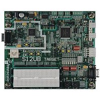
LFEBS12UB Freescale Semiconductor, LFEBS12UB Datasheet - Page 185

LFEBS12UB
Manufacturer Part Number
LFEBS12UB
Description
KIT STUDENT LEARNING S12 DG128
Manufacturer
Freescale Semiconductor
Specifications of LFEBS12UB
Architecture
8/16-bit
Code Gen Tools Included
Code Warrior
Silicon Manufacturer
Freescale
Core Architecture
S12
Core Sub-architecture
S12
Silicon Core Number
MC9S12
Silicon Family Name
S12D
Kit Contents
HCS12 DG128 Learning Kit
Rohs Compliant
Yes
Lead Free Status / RoHS Status
Lead free / RoHS Compliant
- Current page: 185 of 1328
- Download datasheet (9Mb)
2.4.2.9
If the pin is used as an interrupt input this register holds the interrupt flag after a valid pin event.
2.4.2.10
This register supports the re-routing of the CAN0, CAN4, SPI2-0, SCI7-3, IIC0, TIM and CS[3:0] pins to
alternative ports. This allows a software re-configuration of the pinouts of the different package options
with respect to above peripherals.
2.4.3
2.4.3.1
The BKGD pin is associated with the S12X_BDM and S12X_EBI modules.
During reset, the BKGD pin is used as MODC input.
2.4.3.2
Port A pins PA[7:0] and Port B pins PB[7:0] can be used for either general-purpose I/O with the external
bus interface. In this case Port A and Port B are associated with the external address bus outputs ADDR15-
ADDR8 and ADDR7-ADDR0, respectively. PB0 is the ADDR0 or UDS output.
2.4.3.3
Port C pins PC[7:0] and Port D pins PD[7:0] can be used for either general-purpose I/O with the external
bus interface. In this case Port C and Port D are associated with the external data bus inputs/outputs
DATA15-DATA8 and DATA7-DATA0, respectively.
These pins are configured for reduced input threshold in certain operating modes (refer to S12X_EBI
section).
2.4.3.4
Port E is associated with the external bus control outputs RW, LSTRB, LDS and RE, the free-running clock
outputs ECLK and ECLK2X, as well as with the TAGHI, TAGLO, MODA and MODB and interrupt inputs
IRQ and XIRQ.
Port E pins PE[7:2] can be used for either general-purpose I/O or with the alternative functions.
Port E pin PE[7] can be used for either general-purpose I/O or as the free-running clock ECLKX2 output
running at the Core Clock rate. The clock output is always enabled in emulation modes.
Freescale Semiconductor
Pins and Ports
Interrupt flag register (PIFx)
Module routing register (MODRR, PTRRR, PTLRR, PTFRR)
BKGD pin
Port A, B
Port C, D
Port E
Please refer to the SOC Guide to determine the pin availability in the
different package options.
MC9S12XE-Family Reference Manual , Rev. 1.23
NOTE
Chapter 2 Port Integration Module (S12XEPIMV1)
185
Related parts for LFEBS12UB
Image
Part Number
Description
Manufacturer
Datasheet
Request
R
Part Number:
Description:
Manufacturer:
Freescale Semiconductor, Inc
Datasheet:
Part Number:
Description:
Manufacturer:
Freescale Semiconductor, Inc
Datasheet:
Part Number:
Description:
Manufacturer:
Freescale Semiconductor, Inc
Datasheet:
Part Number:
Description:
Manufacturer:
Freescale Semiconductor, Inc
Datasheet:
Part Number:
Description:
Manufacturer:
Freescale Semiconductor, Inc
Datasheet:
Part Number:
Description:
Manufacturer:
Freescale Semiconductor, Inc
Datasheet:
Part Number:
Description:
Manufacturer:
Freescale Semiconductor, Inc
Datasheet:
Part Number:
Description:
Manufacturer:
Freescale Semiconductor, Inc
Datasheet:
Part Number:
Description:
Manufacturer:
Freescale Semiconductor, Inc
Datasheet:
Part Number:
Description:
Manufacturer:
Freescale Semiconductor, Inc
Datasheet:
Part Number:
Description:
Manufacturer:
Freescale Semiconductor, Inc
Datasheet:
Part Number:
Description:
Manufacturer:
Freescale Semiconductor, Inc
Datasheet:
Part Number:
Description:
Manufacturer:
Freescale Semiconductor, Inc
Datasheet:
Part Number:
Description:
Manufacturer:
Freescale Semiconductor, Inc
Datasheet:
Part Number:
Description:
Manufacturer:
Freescale Semiconductor, Inc
Datasheet:


