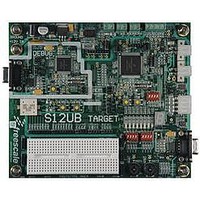
LFEBS12UB Freescale Semiconductor, LFEBS12UB Datasheet - Page 158

LFEBS12UB
Manufacturer Part Number
LFEBS12UB
Description
KIT STUDENT LEARNING S12 DG128
Manufacturer
Freescale Semiconductor
Specifications of LFEBS12UB
Architecture
8/16-bit
Code Gen Tools Included
Code Warrior
Silicon Manufacturer
Freescale
Core Architecture
S12
Core Sub-architecture
S12
Silicon Core Number
MC9S12
Silicon Family Name
S12D
Kit Contents
HCS12 DG128 Learning Kit
Rohs Compliant
Yes
Lead Free Status / RoHS Status
Lead free / RoHS Compliant
- Current page: 158 of 1328
- Download datasheet (9Mb)
1. Read: Anytime.
1. Read: Anytime.
Chapter 2 Port Integration Module (S12XEPIMV1)
2.3.67
2.3.68
158
Address 0x026E
Address 0x026F
Write: Anytime.
Write: Anytime.
Read: Anytime.
Field
Field
PIEJ
PIFJ
Reset
Reset
7-0
7-0
W
W
R
R
Port J interrupt enable—
This register disables or enables on a per-pin basis the edge sensitive external interrupt associated with Port J.
1 Interrupt is enabled.
0 Interrupt is disabled (interrupt flag masked).
Port J interrupt flag—
Each flag is set by an active edge on the associated input pin. This could be a rising or a falling edge based on the
state of the PPSJ register. To clear this flag, write logic level 1 to the corresponding bit in the PIFJ register. Writing
a 0 has no effect.
1 Active edge on the associated bit has occurred (an interrupt will occur if the associated enable bit is set).
0 No active edge pending.
PIEJ7
PIFJ7
Port J Interrupt Enable Register (PIEJ)
Port J Interrupt Flag Register (PIFJ)
0
0
7
7
PIEJ6
PIFJ6
0
0
6
6
Figure 2-65. Port J Interrupt Enable Register (PIEJ)
Figure 2-66. Port J Interrupt Flag Register (PIFJ)
Table 2-63. PPSP Register Field Descriptions
Table 2-64. PPSP Register Field Descriptions
MC9S12XE-Family Reference Manual , Rev. 1.23
PIEJ5
PIFJ5
0
0
5
5
PIEJ4
PIFJ4
0
0
4
4
Description
Description
PIEJ3
PIFJ3
3
0
3
0
PIEJ2
PIFJ2
0
0
2
2
Access: User read/write
Access: User read/write
Freescale Semiconductor
PIEJ1
PIFJ1
0
0
1
1
PIEJ0
PIFJ0
0
0
0
0
(1)
(1)
Related parts for LFEBS12UB
Image
Part Number
Description
Manufacturer
Datasheet
Request
R
Part Number:
Description:
Manufacturer:
Freescale Semiconductor, Inc
Datasheet:
Part Number:
Description:
Manufacturer:
Freescale Semiconductor, Inc
Datasheet:
Part Number:
Description:
Manufacturer:
Freescale Semiconductor, Inc
Datasheet:
Part Number:
Description:
Manufacturer:
Freescale Semiconductor, Inc
Datasheet:
Part Number:
Description:
Manufacturer:
Freescale Semiconductor, Inc
Datasheet:
Part Number:
Description:
Manufacturer:
Freescale Semiconductor, Inc
Datasheet:
Part Number:
Description:
Manufacturer:
Freescale Semiconductor, Inc
Datasheet:
Part Number:
Description:
Manufacturer:
Freescale Semiconductor, Inc
Datasheet:
Part Number:
Description:
Manufacturer:
Freescale Semiconductor, Inc
Datasheet:
Part Number:
Description:
Manufacturer:
Freescale Semiconductor, Inc
Datasheet:
Part Number:
Description:
Manufacturer:
Freescale Semiconductor, Inc
Datasheet:
Part Number:
Description:
Manufacturer:
Freescale Semiconductor, Inc
Datasheet:
Part Number:
Description:
Manufacturer:
Freescale Semiconductor, Inc
Datasheet:
Part Number:
Description:
Manufacturer:
Freescale Semiconductor, Inc
Datasheet:
Part Number:
Description:
Manufacturer:
Freescale Semiconductor, Inc
Datasheet:


