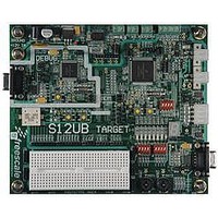
LFEBS12UB Freescale Semiconductor, LFEBS12UB Datasheet - Page 182

LFEBS12UB
Manufacturer Part Number
LFEBS12UB
Description
KIT STUDENT LEARNING S12 DG128
Manufacturer
Freescale Semiconductor
Specifications of LFEBS12UB
Architecture
8/16-bit
Code Gen Tools Included
Code Warrior
Silicon Manufacturer
Freescale
Core Architecture
S12
Core Sub-architecture
S12
Silicon Core Number
MC9S12
Silicon Family Name
S12D
Kit Contents
HCS12 DG128 Learning Kit
Rohs Compliant
Yes
Lead Free Status / RoHS Status
Lead free / RoHS Compliant
- Current page: 182 of 1328
- Download datasheet (9Mb)
Chapter 2 Port Integration Module (S12XEPIMV1)
This register configures the re-routing of SCI3, IIC0, CS[3:0] on alternative ports.
2.4
2.4.1
Each pin except PE0, PE1, and BKGD can act as general purpose I/O. In addition each pin can act as an
output from the external bus interface module or a peripheral module or an input to the external bus
interface module or a peripheral module.
2.4.2
A set of configuration registers is common to all ports with exceptions in the expanded bus interface and
ATD ports
not become active.
This device does not become active while the port is used as a push-pull output.
182
Functional Description
(Table
General
Registers
2-103). All registers can be written at any time, however a specific configuration might
Module
SCI3
CS3
CS2
CS1
CS0
IIC0
MC9S12XE-Family Reference Manual , Rev. 1.23
Example 2-1. Selecting a pull-up device
Table 2-102. Port F Routing Summary
5
0
1
x
x
x
x
x
x
x
x
x
x
4
x
x
0
1
x
x
x
x
x
x
x
x
PTFRR
3
x
x
x
x
0
1
x
x
x
x
x
x
2
x
x
x
x
x
x
0
1
x
x
x
x
1
0
1
x
x
x
x
x
x
x
x
x
x
0
x
x
x
x
x
x
x
x
x
x
0
1
TXD
PM7
SCL
PF7
PF5
PF3
PF2
PF1
PF0
PJ7
PJ0
PJ5
PJ2
PJ4
CS
Related Pins
RXD
PM6
SDA
PF6
PF4
PJ6
Freescale Semiconductor
Related parts for LFEBS12UB
Image
Part Number
Description
Manufacturer
Datasheet
Request
R
Part Number:
Description:
Manufacturer:
Freescale Semiconductor, Inc
Datasheet:
Part Number:
Description:
Manufacturer:
Freescale Semiconductor, Inc
Datasheet:
Part Number:
Description:
Manufacturer:
Freescale Semiconductor, Inc
Datasheet:
Part Number:
Description:
Manufacturer:
Freescale Semiconductor, Inc
Datasheet:
Part Number:
Description:
Manufacturer:
Freescale Semiconductor, Inc
Datasheet:
Part Number:
Description:
Manufacturer:
Freescale Semiconductor, Inc
Datasheet:
Part Number:
Description:
Manufacturer:
Freescale Semiconductor, Inc
Datasheet:
Part Number:
Description:
Manufacturer:
Freescale Semiconductor, Inc
Datasheet:
Part Number:
Description:
Manufacturer:
Freescale Semiconductor, Inc
Datasheet:
Part Number:
Description:
Manufacturer:
Freescale Semiconductor, Inc
Datasheet:
Part Number:
Description:
Manufacturer:
Freescale Semiconductor, Inc
Datasheet:
Part Number:
Description:
Manufacturer:
Freescale Semiconductor, Inc
Datasheet:
Part Number:
Description:
Manufacturer:
Freescale Semiconductor, Inc
Datasheet:
Part Number:
Description:
Manufacturer:
Freescale Semiconductor, Inc
Datasheet:
Part Number:
Description:
Manufacturer:
Freescale Semiconductor, Inc
Datasheet:


