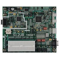
LFEBS12UB Freescale Semiconductor, LFEBS12UB Datasheet - Page 1240

LFEBS12UB
Manufacturer Part Number
LFEBS12UB
Description
KIT STUDENT LEARNING S12 DG128
Manufacturer
Freescale Semiconductor
Specifications of LFEBS12UB
Architecture
8/16-bit
Code Gen Tools Included
Code Warrior
Silicon Manufacturer
Freescale
Core Architecture
S12
Core Sub-architecture
S12
Silicon Core Number
MC9S12
Silicon Family Name
S12D
Kit Contents
HCS12 DG128 Learning Kit
Rohs Compliant
Yes
Lead Free Status / RoHS Status
Lead free / RoHS Compliant
- Current page: 1240 of 1328
- Download datasheet (9Mb)
Appendix A Electrical Characteristics
A.6.3
Phase Locked Loop
A.6.3.1
Jitter Information
With each transition of the clock f
, the deviation from the reference clock f
is measured and input
cmp
ref
voltage to the VCO is adjusted accordingly.The adjustment is done continuously with no abrupt changes
in the clock output frequency. Noise, voltage, temperature and other factors cause slight variations in the
control loop resulting in a clock jitter. This jitter affects the real minimum and maximum clock periods as
illustrated in
Figure
A-5.
1
2
3
N-1
N
0
t
min1
t
nom
t
max1
t
minN
t
maxN
Figure A-5. Jitter Definitions
The relative deviation of t
is at its maximum for one clock period, and decreases towards zero for larger
nom
number of clock periods (N).
MC9S12XE-Family Reference Manual , Rev. 1.23
1240
Freescale Semiconductor
Related parts for LFEBS12UB
Image
Part Number
Description
Manufacturer
Datasheet
Request
R
Part Number:
Description:
Manufacturer:
Freescale Semiconductor, Inc
Datasheet:
Part Number:
Description:
Manufacturer:
Freescale Semiconductor, Inc
Datasheet:
Part Number:
Description:
Manufacturer:
Freescale Semiconductor, Inc
Datasheet:
Part Number:
Description:
Manufacturer:
Freescale Semiconductor, Inc
Datasheet:
Part Number:
Description:
Manufacturer:
Freescale Semiconductor, Inc
Datasheet:
Part Number:
Description:
Manufacturer:
Freescale Semiconductor, Inc
Datasheet:
Part Number:
Description:
Manufacturer:
Freescale Semiconductor, Inc
Datasheet:
Part Number:
Description:
Manufacturer:
Freescale Semiconductor, Inc
Datasheet:
Part Number:
Description:
Manufacturer:
Freescale Semiconductor, Inc
Datasheet:
Part Number:
Description:
Manufacturer:
Freescale Semiconductor, Inc
Datasheet:
Part Number:
Description:
Manufacturer:
Freescale Semiconductor, Inc
Datasheet:
Part Number:
Description:
Manufacturer:
Freescale Semiconductor, Inc
Datasheet:
Part Number:
Description:
Manufacturer:
Freescale Semiconductor, Inc
Datasheet:
Part Number:
Description:
Manufacturer:
Freescale Semiconductor, Inc
Datasheet:
Part Number:
Description:
Manufacturer:
Freescale Semiconductor, Inc
Datasheet:


