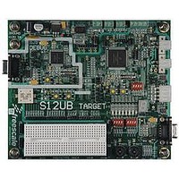
LFEBS12UB Freescale Semiconductor, LFEBS12UB Datasheet - Page 539

LFEBS12UB
Manufacturer Part Number
LFEBS12UB
Description
KIT STUDENT LEARNING S12 DG128
Manufacturer
Freescale Semiconductor
Specifications of LFEBS12UB
Architecture
8/16-bit
Code Gen Tools Included
Code Warrior
Silicon Manufacturer
Freescale
Core Architecture
S12
Core Sub-architecture
S12
Silicon Core Number
MC9S12
Silicon Family Name
S12D
Kit Contents
HCS12 DG128 Learning Kit
Rohs Compliant
Yes
Lead Free Status / RoHS Status
Lead free / RoHS Compliant
- Current page: 539 of 1328
- Download datasheet (9Mb)
14.3.2.4
Read or write: Anytime
All bits reset to zero.
14.3.2.5
Freescale Semiconductor
Module Base + 0x0003
Module Base + 0x0004
OC7M[7:0]
OC7D[7:0]
Because of an order from the United States International Trade Commission, BGA-packaged product lines and partnumbers
Reset
Reset
indicated here currently are not available from Freescale for import or sale in the United States prior to September 2010
Field
Field
7:0
7:0
W
W
R
R
TCNT15
OC7D7
Output Compare Mask Action for Channel 7:0
A channel 7 event, which can be a counter overflow when TTOV[7] is set or a successful output compare
on channel 7, overrides any channel 6:0 compares. For each OC7M bit that is set,the output compare
action reflects the corresponding OC7D bit.
0 The corresponding OC7Dx bit in the output compare 7 data register will not be transferred to the timer port on
1 The corresponding OC7Dx bit in the output compare 7 data register will be transferred to the timer port on a
Note: The corresponding channel must also be setup for output compare (IOSx = 1 andOCPDx = 0) for data to
Output Compare 7 Data Bits — A channel 7 event, which can be a counter overflow when TTOV[7] is set or A
channel 7 output compare can cause bits in the output compare 7 data register to transfer to the timer port data
register depending on the output compare 7 mask register.
Output Compare 7 Data Register (OC7D)
Timer Count Register (TCNT)
15
0
0
7
a channel 7 event, even if the corresponding pin is setup for output compare.
channel 7 event.
be transferred from the output compare 7 data register to the timer port.
TCNT14
OC7D6
14
0
0
6
Figure 14-6. Output Compare 7 Data Register (OC7D)
Figure 14-7. Timer Count Register High (TCNT)
MC9S12XE-Family Reference Manual Rev. 1.23
Table 14-4. OC7M Field Descriptions
Table 14-5. OC7D Field Descriptions
TCNT13
OC7D5
13
5
0
0
TCNT12
OC7D4
12
0
0
4
Description
Description
TCNT11
OC7D3
11
0
0
3
Chapter 14 Enhanced Capture Timer (ECT16B8CV3)
TCNT10
OC7D2
10
2
0
0
OC7D1
TCNT9
0
0
1
9
OC7D0
TCNT8
0
0
0
8
539
Related parts for LFEBS12UB
Image
Part Number
Description
Manufacturer
Datasheet
Request
R
Part Number:
Description:
Manufacturer:
Freescale Semiconductor, Inc
Datasheet:
Part Number:
Description:
Manufacturer:
Freescale Semiconductor, Inc
Datasheet:
Part Number:
Description:
Manufacturer:
Freescale Semiconductor, Inc
Datasheet:
Part Number:
Description:
Manufacturer:
Freescale Semiconductor, Inc
Datasheet:
Part Number:
Description:
Manufacturer:
Freescale Semiconductor, Inc
Datasheet:
Part Number:
Description:
Manufacturer:
Freescale Semiconductor, Inc
Datasheet:
Part Number:
Description:
Manufacturer:
Freescale Semiconductor, Inc
Datasheet:
Part Number:
Description:
Manufacturer:
Freescale Semiconductor, Inc
Datasheet:
Part Number:
Description:
Manufacturer:
Freescale Semiconductor, Inc
Datasheet:
Part Number:
Description:
Manufacturer:
Freescale Semiconductor, Inc
Datasheet:
Part Number:
Description:
Manufacturer:
Freescale Semiconductor, Inc
Datasheet:
Part Number:
Description:
Manufacturer:
Freescale Semiconductor, Inc
Datasheet:
Part Number:
Description:
Manufacturer:
Freescale Semiconductor, Inc
Datasheet:
Part Number:
Description:
Manufacturer:
Freescale Semiconductor, Inc
Datasheet:
Part Number:
Description:
Manufacturer:
Freescale Semiconductor, Inc
Datasheet:


