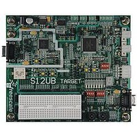
LFEBS12UB Freescale Semiconductor, LFEBS12UB Datasheet - Page 165

LFEBS12UB
Manufacturer Part Number
LFEBS12UB
Description
KIT STUDENT LEARNING S12 DG128
Manufacturer
Freescale Semiconductor
Specifications of LFEBS12UB
Architecture
8/16-bit
Code Gen Tools Included
Code Warrior
Silicon Manufacturer
Freescale
Core Architecture
S12
Core Sub-architecture
S12
Silicon Core Number
MC9S12
Silicon Family Name
S12D
Kit Contents
HCS12 DG128 Learning Kit
Rohs Compliant
Yes
Lead Free Status / RoHS Status
Lead free / RoHS Compliant
- Current page: 165 of 1328
- Download datasheet (9Mb)
1. Read: Anytime.
2.3.80
Freescale Semiconductor
DDR1AD1
Address 0x027B
Write: Anytime.
Field
Reset
7-0
W
R
DDR1AD17
Port AD1 data direction—
This register controls the data direction of pins 7 through 0.
1 Associated pin is configured as output.
0 Associated pin is configured as input.
Port AD1 Data Direction Register 1 (DDR1AD1)
0
7
Due to internal synchronization circuits, it can take up to 2 bus clock cycles
until the correct value is read on PT0AD1 registers, when changing the
DDR0AD1 register.
To use the digital input function on Port AD1 the ATD Digital Input Enable
Register (ATD1DIEN1) has to be set to logic level “1”.
Due to internal synchronization circuits, it can take up to 2 bus clock cycles
until the correct value is read on PT0AD1 registers, when changing the
DDR1AD1 register.
To use the digital input function on Port AD1 the ATD Digital Input Enable
Register (ATD1DIEN1) has to be set to logic level “1”.
DDR1AD16
Figure 2-78. Port AD1 Data Direction Register 1 (DDR1AD1)
0
6
Table 2-76. DDR1AD1 Register Field Descriptions
MC9S12XE-Family Reference Manual , Rev. 1.23
DDR1AD15
0
5
DDR1AD14
NOTE
NOTE
NOTE
NOTE
0
4
Description
DDR1AD13
3
0
Chapter 2 Port Integration Module (S12XEPIMV1)
DDR1AD12
0
2
DDR1AD11
Access: User read/write
0
1
DDR1AD10
0
0
165
(1)
Related parts for LFEBS12UB
Image
Part Number
Description
Manufacturer
Datasheet
Request
R
Part Number:
Description:
Manufacturer:
Freescale Semiconductor, Inc
Datasheet:
Part Number:
Description:
Manufacturer:
Freescale Semiconductor, Inc
Datasheet:
Part Number:
Description:
Manufacturer:
Freescale Semiconductor, Inc
Datasheet:
Part Number:
Description:
Manufacturer:
Freescale Semiconductor, Inc
Datasheet:
Part Number:
Description:
Manufacturer:
Freescale Semiconductor, Inc
Datasheet:
Part Number:
Description:
Manufacturer:
Freescale Semiconductor, Inc
Datasheet:
Part Number:
Description:
Manufacturer:
Freescale Semiconductor, Inc
Datasheet:
Part Number:
Description:
Manufacturer:
Freescale Semiconductor, Inc
Datasheet:
Part Number:
Description:
Manufacturer:
Freescale Semiconductor, Inc
Datasheet:
Part Number:
Description:
Manufacturer:
Freescale Semiconductor, Inc
Datasheet:
Part Number:
Description:
Manufacturer:
Freescale Semiconductor, Inc
Datasheet:
Part Number:
Description:
Manufacturer:
Freescale Semiconductor, Inc
Datasheet:
Part Number:
Description:
Manufacturer:
Freescale Semiconductor, Inc
Datasheet:
Part Number:
Description:
Manufacturer:
Freescale Semiconductor, Inc
Datasheet:
Part Number:
Description:
Manufacturer:
Freescale Semiconductor, Inc
Datasheet:


