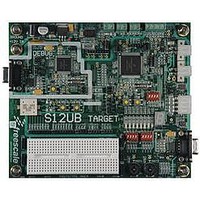
LFEBS12UB Freescale Semiconductor, LFEBS12UB Datasheet - Page 632

LFEBS12UB
Manufacturer Part Number
LFEBS12UB
Description
KIT STUDENT LEARNING S12 DG128
Manufacturer
Freescale Semiconductor
Specifications of LFEBS12UB
Architecture
8/16-bit
Code Gen Tools Included
Code Warrior
Silicon Manufacturer
Freescale
Core Architecture
S12
Core Sub-architecture
S12
Silicon Core Number
MC9S12
Silicon Family Name
S12D
Kit Contents
HCS12 DG128 Learning Kit
Rohs Compliant
Yes
Lead Free Status / RoHS Status
Lead free / RoHS Compliant
- Current page: 632 of 1328
- Download datasheet (9Mb)
1. Read: Anytime
Chapter 16 Freescale’s Scalable Controller Area Network (S12MSCANV3)
16.3.3
The following section details the organization of the receive and transmit message buffers and the
associated control registers.
To simplify the programmer interface, the receive and transmit message buffers have the same outline.
Each message buffer allocates 16 bytes in the memory map containing a 13 byte data structure.
An additional transmit buffer priority register (TBPR) is defined for the transmit buffers. Within the last
two bytes of this memory map, the MSCAN stores a special 16-bit time stamp, which is sampled from an
internal timer after successful transmission or reception of a message. This feature is only available for
transmit and receiver buffers, if the TIME bit is set (see
(CANCTL0)”).
The time stamp register is written by the MSCAN. The CPU can only read these registers.
632
Write: Anytime in initialization mode (INITRQ = 1 and INITAK = 1)
AM[7:0]
Field
7-0
Programmer’s Model of Message Storage
Acceptance Mask Bits — If a particular bit in this register is cleared, this indicates that the corresponding bit in
the identifier acceptance register must be the same as its identifier bit before a match is detected. The message
is accepted if all such bits match. If a bit is set, it indicates that the state of the corresponding bit in the identifier
acceptance register does not affect whether or not the message is accepted.
0 Match corresponding acceptance code register and identifier bits
1 Ignore corresponding acceptance code register bit
Table 16-25. CANIDMR4–CANIDMR7 Register Field Descriptions
MC9S12XE-Family Reference Manual , Rev. 1.23
Description
Section 16.3.2.1, “MSCAN Control Register 0
Freescale Semiconductor
Related parts for LFEBS12UB
Image
Part Number
Description
Manufacturer
Datasheet
Request
R
Part Number:
Description:
Manufacturer:
Freescale Semiconductor, Inc
Datasheet:
Part Number:
Description:
Manufacturer:
Freescale Semiconductor, Inc
Datasheet:
Part Number:
Description:
Manufacturer:
Freescale Semiconductor, Inc
Datasheet:
Part Number:
Description:
Manufacturer:
Freescale Semiconductor, Inc
Datasheet:
Part Number:
Description:
Manufacturer:
Freescale Semiconductor, Inc
Datasheet:
Part Number:
Description:
Manufacturer:
Freescale Semiconductor, Inc
Datasheet:
Part Number:
Description:
Manufacturer:
Freescale Semiconductor, Inc
Datasheet:
Part Number:
Description:
Manufacturer:
Freescale Semiconductor, Inc
Datasheet:
Part Number:
Description:
Manufacturer:
Freescale Semiconductor, Inc
Datasheet:
Part Number:
Description:
Manufacturer:
Freescale Semiconductor, Inc
Datasheet:
Part Number:
Description:
Manufacturer:
Freescale Semiconductor, Inc
Datasheet:
Part Number:
Description:
Manufacturer:
Freescale Semiconductor, Inc
Datasheet:
Part Number:
Description:
Manufacturer:
Freescale Semiconductor, Inc
Datasheet:
Part Number:
Description:
Manufacturer:
Freescale Semiconductor, Inc
Datasheet:
Part Number:
Description:
Manufacturer:
Freescale Semiconductor, Inc
Datasheet:


