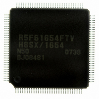
DF61654N50FTV Renesas Electronics America, DF61654N50FTV Datasheet - Page 895

DF61654N50FTV
Manufacturer Part Number
DF61654N50FTV
Description
IC H8SX/1654 MCU FLASH 120TQFP
Manufacturer
Renesas Electronics America
Series
H8® H8SX/1600r
Datasheet
1.DF61653N50FTV.pdf
(1020 pages)
Specifications of DF61654N50FTV
Core Processor
H8SX
Core Size
32-Bit
Speed
50MHz
Connectivity
I²C, IrDA, SCI, SmartCard, USB
Peripherals
DMA, PWM, WDT
Number Of I /o
75
Program Memory Size
512KB (512K x 8)
Program Memory Type
FLASH
Ram Size
40K x 8
Voltage - Supply (vcc/vdd)
3 V ~ 3.6 V
Data Converters
A/D 8x10b; D/A 2x8b
Oscillator Type
External
Operating Temperature
-20°C ~ 75°C
Package / Case
120-TQFP, 120-VQFP
For Use With
HS0005KCU11H - EMULATOR E10A-USB H8S(X),SH2(A)3DK1657 - DEV EVAL KIT FOR H8SX/1657
Lead Free Status / RoHS Status
Lead free / RoHS Compliant
Eeprom Size
-
Available stocks
Company
Part Number
Manufacturer
Quantity
Price
Company:
Part Number:
DF61654N50FTV
Manufacturer:
Renesas Electronics America
Quantity:
10 000
- Current page: 895 of 1020
- Download datasheet (6Mb)
21.1
The clock pulse generator has the following register.
• System clock control register (SCKCR)
21.1.1
SCKCR controls φ clock output and frequencies of the system, peripheral module, and external
bus clocks, and selects the φ clock to be output.
Bit
15
14
Bit
Bit Name
Initial Value
R/W
Bit
Bit Name
Initial Value
R/W
Register Description
System Clock Control Register (SCKCR)
Bit Name
PSTOP1
PSTOP1
R/W
R/W
15
7
0
0
Initial
Value
0
0
PCK2
R/W
R/W
14
0
6
0
R/W
R/W
R/W
POSEL1
PCK1
R/W
R/W
13
0
5
1
Description
φ Clock Output Enable
Controls φ output on PA7.
•
0: φ output
1: Fixed high
•
X: Fixed high
•
X: Hi-Z
Reserved
Although this bit is readable/writable, only 0 should be
written to.
PCK0
Normal operation
Software standby mode
Hardware standby mode
R/W
R/W
12
0
4
0
R/W
R/W
11
0
3
0
Rev.1.00 Sep. 08, 2005 Page 845 of 966
Section 21 Clock Pulse Generator
BCK2
ICK2
R/W
R/W
10
0
2
0
BCK1
ICK1
R/W
R/W
9
1
1
1
REJ09B0219-0100
BCK0
ICK0
R/W
R/W
8
0
0
0
Related parts for DF61654N50FTV
Image
Part Number
Description
Manufacturer
Datasheet
Request
R

Part Number:
Description:
KIT STARTER FOR M16C/29
Manufacturer:
Renesas Electronics America
Datasheet:

Part Number:
Description:
KIT STARTER FOR R8C/2D
Manufacturer:
Renesas Electronics America
Datasheet:

Part Number:
Description:
R0K33062P STARTER KIT
Manufacturer:
Renesas Electronics America
Datasheet:

Part Number:
Description:
KIT STARTER FOR R8C/23 E8A
Manufacturer:
Renesas Electronics America
Datasheet:

Part Number:
Description:
KIT STARTER FOR R8C/25
Manufacturer:
Renesas Electronics America
Datasheet:

Part Number:
Description:
KIT STARTER H8S2456 SHARPE DSPLY
Manufacturer:
Renesas Electronics America
Datasheet:

Part Number:
Description:
KIT STARTER FOR R8C38C
Manufacturer:
Renesas Electronics America
Datasheet:

Part Number:
Description:
KIT STARTER FOR R8C35C
Manufacturer:
Renesas Electronics America
Datasheet:

Part Number:
Description:
KIT STARTER FOR R8CL3AC+LCD APPS
Manufacturer:
Renesas Electronics America
Datasheet:

Part Number:
Description:
KIT STARTER FOR RX610
Manufacturer:
Renesas Electronics America
Datasheet:

Part Number:
Description:
KIT STARTER FOR R32C/118
Manufacturer:
Renesas Electronics America
Datasheet:

Part Number:
Description:
KIT DEV RSK-R8C/26-29
Manufacturer:
Renesas Electronics America
Datasheet:

Part Number:
Description:
KIT STARTER FOR SH7124
Manufacturer:
Renesas Electronics America
Datasheet:

Part Number:
Description:
KIT STARTER FOR H8SX/1622
Manufacturer:
Renesas Electronics America
Datasheet:

Part Number:
Description:
KIT DEV FOR SH7203
Manufacturer:
Renesas Electronics America
Datasheet:


