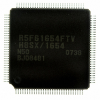
DF61654N50FTV Renesas Electronics America, DF61654N50FTV Datasheet - Page 31

DF61654N50FTV
Manufacturer Part Number
DF61654N50FTV
Description
IC H8SX/1654 MCU FLASH 120TQFP
Manufacturer
Renesas Electronics America
Series
H8® H8SX/1600r
Datasheet
1.DF61653N50FTV.pdf
(1020 pages)
Specifications of DF61654N50FTV
Core Processor
H8SX
Core Size
32-Bit
Speed
50MHz
Connectivity
I²C, IrDA, SCI, SmartCard, USB
Peripherals
DMA, PWM, WDT
Number Of I /o
75
Program Memory Size
512KB (512K x 8)
Program Memory Type
FLASH
Ram Size
40K x 8
Voltage - Supply (vcc/vdd)
3 V ~ 3.6 V
Data Converters
A/D 8x10b; D/A 2x8b
Oscillator Type
External
Operating Temperature
-20°C ~ 75°C
Package / Case
120-TQFP, 120-VQFP
For Use With
HS0005KCU11H - EMULATOR E10A-USB H8S(X),SH2(A)3DK1657 - DEV EVAL KIT FOR H8SX/1657
Lead Free Status / RoHS Status
Lead free / RoHS Compliant
Eeprom Size
-
Available stocks
Company
Part Number
Manufacturer
Quantity
Price
Company:
Part Number:
DF61654N50FTV
Manufacturer:
Renesas Electronics America
Quantity:
10 000
- Current page: 31 of 1020
- Download datasheet (6Mb)
Figure 6.32 Access Timing of 3 Address Cycles (ADDEX = 1) ................................................ 202
Figure 6.33 Read Strobe Timing................................................................................................. 204
Figure 6.34 Chip Select (CS) Assertion Period Extension Timing in Data Cycle ...................... 205
Figure 6.35 Consecutive Read Accesses to Same Area
Figure 6.36 DACK Signal Output Timing.................................................................................. 207
Figure 6.37 Example of Idle Cycle Operation (Consecutive Reads in Different Areas) ............ 210
Figure 6.38 Example of Idle Cycle Operation (Write after Read) .............................................. 211
Figure 6.39 Example of Idle Cycle Operation (Read after Write) .............................................. 212
Figure 6.40 Example of Idle Cycle Operation (Write after Single Address Transfer Write)...... 213
Figure 6.41 Idle Cycle Insertion Example .................................................................................. 214
Figure 6.42 Relationship between Chip Select (CS) and Read (RD).......................................... 215
Figure 6.43 Bus Released State Transition Timing .................................................................... 220
Figure 6.44 Example of Timing when Write Data Buffer Function is Used .............................. 222
Figure 6.45 Example of Timing when Peripheral Module
Section 7 DMA Controller (DMAC)
Figure 7.1 Block Diagram of DMAC ......................................................................................... 231
Figure 7.2 Example of Signal Timing in Dual Address Mode.................................................... 256
Figure 7.3 Operations in Dual Address Mode ............................................................................ 256
Figure 7.4 Data Flow in Single Address Mode........................................................................... 257
Figure 7.5 Example of Signal Timing in Single Address Mode ................................................. 258
Figure 7.6 Operations in Single Address Mode.......................................................................... 258
Figure 7.7 Example of Signal Timing in Normal Transfer Mode............................................... 259
Figure 7.8 Operations in Normal Transfer Mode ....................................................................... 260
Figure 7.9 Operations in Repeat Transfer Mode......................................................................... 261
Figure 7.10 Operations in Block Transfer Mode ........................................................................ 262
Figure 7.11 Operation in Single Address Mode in Block Transfer Mode
Figure 7.12 Operation in Dual Address Mode in Block Transfer Mode
Figure 7.13 Example of Timing in Cycle Stealing Mode ........................................................... 267
Figure 7.14 Example of Timing in Burst Mode.......................................................................... 267
Figure 7.15 Example of Extended Repeat Area Operation......................................................... 269
Figure 7.16 Example of Extended Repeat Area Function in Block Transfer Mode ................... 270
Figure 7.17 Address Update Method .......................................................................................... 271
Figure 7.18 Operation of Offset Addition................................................................................... 272
Figure 7.19 XY Conversion Operation Using Offset Addition in Repeat Transfer Mode.......... 273
Figure 7.20 XY Conversion Flowchart Using Offset Addition in Repeat Transfer Mode ......... 274
Figure 7.21 Procedure for Changing Register Setting For Channel being Transferred .............. 278
(Address/Data Multiplexed I/O Space).................................................................... 206
(Block Area Specified) ............................................................................................ 262
Write Data Buffer Function is Used ....................................................................... 223
(Block Area Not Specified) .................................................................................... 263
Rev.1.00 Sep. 08, 2005 Page xxix of xlviii
Related parts for DF61654N50FTV
Image
Part Number
Description
Manufacturer
Datasheet
Request
R

Part Number:
Description:
KIT STARTER FOR M16C/29
Manufacturer:
Renesas Electronics America
Datasheet:

Part Number:
Description:
KIT STARTER FOR R8C/2D
Manufacturer:
Renesas Electronics America
Datasheet:

Part Number:
Description:
R0K33062P STARTER KIT
Manufacturer:
Renesas Electronics America
Datasheet:

Part Number:
Description:
KIT STARTER FOR R8C/23 E8A
Manufacturer:
Renesas Electronics America
Datasheet:

Part Number:
Description:
KIT STARTER FOR R8C/25
Manufacturer:
Renesas Electronics America
Datasheet:

Part Number:
Description:
KIT STARTER H8S2456 SHARPE DSPLY
Manufacturer:
Renesas Electronics America
Datasheet:

Part Number:
Description:
KIT STARTER FOR R8C38C
Manufacturer:
Renesas Electronics America
Datasheet:

Part Number:
Description:
KIT STARTER FOR R8C35C
Manufacturer:
Renesas Electronics America
Datasheet:

Part Number:
Description:
KIT STARTER FOR R8CL3AC+LCD APPS
Manufacturer:
Renesas Electronics America
Datasheet:

Part Number:
Description:
KIT STARTER FOR RX610
Manufacturer:
Renesas Electronics America
Datasheet:

Part Number:
Description:
KIT STARTER FOR R32C/118
Manufacturer:
Renesas Electronics America
Datasheet:

Part Number:
Description:
KIT DEV RSK-R8C/26-29
Manufacturer:
Renesas Electronics America
Datasheet:

Part Number:
Description:
KIT STARTER FOR SH7124
Manufacturer:
Renesas Electronics America
Datasheet:

Part Number:
Description:
KIT STARTER FOR H8SX/1622
Manufacturer:
Renesas Electronics America
Datasheet:

Part Number:
Description:
KIT DEV FOR SH7203
Manufacturer:
Renesas Electronics America
Datasheet:


