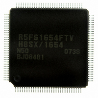
DF61654N50FTV Renesas Electronics America, DF61654N50FTV Datasheet - Page 211

DF61654N50FTV
Manufacturer Part Number
DF61654N50FTV
Description
IC H8SX/1654 MCU FLASH 120TQFP
Manufacturer
Renesas Electronics America
Series
H8® H8SX/1600r
Datasheet
1.DF61653N50FTV.pdf
(1020 pages)
Specifications of DF61654N50FTV
Core Processor
H8SX
Core Size
32-Bit
Speed
50MHz
Connectivity
I²C, IrDA, SCI, SmartCard, USB
Peripherals
DMA, PWM, WDT
Number Of I /o
75
Program Memory Size
512KB (512K x 8)
Program Memory Type
FLASH
Ram Size
40K x 8
Voltage - Supply (vcc/vdd)
3 V ~ 3.6 V
Data Converters
A/D 8x10b; D/A 2x8b
Oscillator Type
External
Operating Temperature
-20°C ~ 75°C
Package / Case
120-TQFP, 120-VQFP
For Use With
HS0005KCU11H - EMULATOR E10A-USB H8S(X),SH2(A)3DK1657 - DEV EVAL KIT FOR H8SX/1657
Lead Free Status / RoHS Status
Lead free / RoHS Compliant
Eeprom Size
-
Available stocks
Company
Part Number
Manufacturer
Quantity
Price
Company:
Part Number:
DF61654N50FTV
Manufacturer:
Renesas Electronics America
Quantity:
10 000
- Current page: 211 of 1020
- Download datasheet (6Mb)
Table 6.5
(2)
A bus width of 8 or 16 bits can be selected with ABWCR. An area for which an 8-bit bus is
selected functions as an 8-bit access space and an area for which a 16-bit bus is selected functions
as a 16-bit access space. In addition, the bus width of address/data multiplexed I/O space is 8 bits
or 16 bits, and the bus width for the byte control SRAM space is 16 bits.
The initial state of the bus width is specified by the operating mode.
If all areas are designated as 8-bit access space, 8-bit bus mode is set; if any area is designated as
16-bit access space, 16-bit bus mode is set.
(3)
Though the endian format of this LSI is big endian, data can be converted into little endian format
when reading or writing to the external address space.
Areas 7 to 2 can be specified as either big endian or little endian format by the LE7 to LE2 bits in
ENDIANCR.
The initial state of each area is the big endian format.
Note that the data format for the areas used as a program area or a stack area should be big endian.
Interface
Basic interface
Byte control SRAM interface
Burst ROM interface
Address/data multiplexed I/O
interface
Bus Width
Endian Format
Areas Specifiable for Each Interface
Related
Registers
SRAMCR
BROMCR
MPXCR
0
O
O
O
1
O
O
O
2
O
O
Rev.1.00 Sep. 08, 2005 Page 161 of 966
3
O
O
O
Section 6 Bus Controller (BSC)
Areas
4
O
O
O
5
O
O
O
REJ09B0219-0100
6
O
O
O
7
O
O
O
Related parts for DF61654N50FTV
Image
Part Number
Description
Manufacturer
Datasheet
Request
R

Part Number:
Description:
KIT STARTER FOR M16C/29
Manufacturer:
Renesas Electronics America
Datasheet:

Part Number:
Description:
KIT STARTER FOR R8C/2D
Manufacturer:
Renesas Electronics America
Datasheet:

Part Number:
Description:
R0K33062P STARTER KIT
Manufacturer:
Renesas Electronics America
Datasheet:

Part Number:
Description:
KIT STARTER FOR R8C/23 E8A
Manufacturer:
Renesas Electronics America
Datasheet:

Part Number:
Description:
KIT STARTER FOR R8C/25
Manufacturer:
Renesas Electronics America
Datasheet:

Part Number:
Description:
KIT STARTER H8S2456 SHARPE DSPLY
Manufacturer:
Renesas Electronics America
Datasheet:

Part Number:
Description:
KIT STARTER FOR R8C38C
Manufacturer:
Renesas Electronics America
Datasheet:

Part Number:
Description:
KIT STARTER FOR R8C35C
Manufacturer:
Renesas Electronics America
Datasheet:

Part Number:
Description:
KIT STARTER FOR R8CL3AC+LCD APPS
Manufacturer:
Renesas Electronics America
Datasheet:

Part Number:
Description:
KIT STARTER FOR RX610
Manufacturer:
Renesas Electronics America
Datasheet:

Part Number:
Description:
KIT STARTER FOR R32C/118
Manufacturer:
Renesas Electronics America
Datasheet:

Part Number:
Description:
KIT DEV RSK-R8C/26-29
Manufacturer:
Renesas Electronics America
Datasheet:

Part Number:
Description:
KIT STARTER FOR SH7124
Manufacturer:
Renesas Electronics America
Datasheet:

Part Number:
Description:
KIT STARTER FOR H8SX/1622
Manufacturer:
Renesas Electronics America
Datasheet:

Part Number:
Description:
KIT DEV FOR SH7203
Manufacturer:
Renesas Electronics America
Datasheet:


