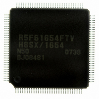
DF61654N50FTV Renesas Electronics America, DF61654N50FTV Datasheet - Page 544

DF61654N50FTV
Manufacturer Part Number
DF61654N50FTV
Description
IC H8SX/1654 MCU FLASH 120TQFP
Manufacturer
Renesas Electronics America
Series
H8® H8SX/1600r
Datasheet
1.DF61653N50FTV.pdf
(1020 pages)
Specifications of DF61654N50FTV
Core Processor
H8SX
Core Size
32-Bit
Speed
50MHz
Connectivity
I²C, IrDA, SCI, SmartCard, USB
Peripherals
DMA, PWM, WDT
Number Of I /o
75
Program Memory Size
512KB (512K x 8)
Program Memory Type
FLASH
Ram Size
40K x 8
Voltage - Supply (vcc/vdd)
3 V ~ 3.6 V
Data Converters
A/D 8x10b; D/A 2x8b
Oscillator Type
External
Operating Temperature
-20°C ~ 75°C
Package / Case
120-TQFP, 120-VQFP
For Use With
HS0005KCU11H - EMULATOR E10A-USB H8S(X),SH2(A)3DK1657 - DEV EVAL KIT FOR H8SX/1657
Lead Free Status / RoHS Status
Lead free / RoHS Compliant
Eeprom Size
-
Available stocks
Company
Part Number
Manufacturer
Quantity
Price
Company:
Part Number:
DF61654N50FTV
Manufacturer:
Renesas Electronics America
Quantity:
10 000
- Current page: 544 of 1020
- Download datasheet (6Mb)
Section 11 Programmable Pulse Generator (PPG)
11.4.5
Figure 11.8 shows a sample procedure for setting up non-overlapping pulse output.
Rev.1.00 Sep. 08, 2005 Page 494 of 966
REJ09B0219-0100
PPG setup
TPU setup
TPU setup
Figure 11.8 Setup Procedure for Non-Overlapping Pulse Output (Example)
Sample Setup Procedure for Non-Overlapping Pulse Output
Set non-overlapping groups
Set counting operation
Select interrupt request
Select TGR functions
Set initial output data
Select output trigger
Enable pulse output
Compare match A?
Non-overlapping
Set TGR values
Set next pulse
Set next pulse
Start counter
pulse output
output data
output data
Yes
No
[1]
[2]
[3]
[4]
[5]
[6]
[7]
[8]
[9]
[10]
[11]
[1]
[2]
[3]
[4]
[5]
[6]
[7]
[8]
[9]
[10] Set the CST bit in TSTR to 1 to start the
[11] At each TGIA interrupt, set the next
Set TIOR to make TGRA and TGRB
output compare registers (with output
disabled).
Set the pulse output trigger cycle in
TGRB and the non-overlapping margin
in TGRA.
Select the counter clock source with bits
TPSC2 to TPSC0 in TCR. Select the
counter clear source with bits CCLR1
and CCLR0.
Enable the TGIA interrupt in TIER. The
DTC or DMAC can also be set up to
transfer data to NDR.
Set the initial output values in PODR.
Set the bits in NDER for the pins to be
used for pulse output to 1.
Select the TPU compare match event to
be used as the pulse output trigger in
PCR.
In PMR, select the groups that will
operate in non-overlapping mode.
Set the next pulse output values in NDR.
TCNT counter.
output values in NDR.
Related parts for DF61654N50FTV
Image
Part Number
Description
Manufacturer
Datasheet
Request
R

Part Number:
Description:
KIT STARTER FOR M16C/29
Manufacturer:
Renesas Electronics America
Datasheet:

Part Number:
Description:
KIT STARTER FOR R8C/2D
Manufacturer:
Renesas Electronics America
Datasheet:

Part Number:
Description:
R0K33062P STARTER KIT
Manufacturer:
Renesas Electronics America
Datasheet:

Part Number:
Description:
KIT STARTER FOR R8C/23 E8A
Manufacturer:
Renesas Electronics America
Datasheet:

Part Number:
Description:
KIT STARTER FOR R8C/25
Manufacturer:
Renesas Electronics America
Datasheet:

Part Number:
Description:
KIT STARTER H8S2456 SHARPE DSPLY
Manufacturer:
Renesas Electronics America
Datasheet:

Part Number:
Description:
KIT STARTER FOR R8C38C
Manufacturer:
Renesas Electronics America
Datasheet:

Part Number:
Description:
KIT STARTER FOR R8C35C
Manufacturer:
Renesas Electronics America
Datasheet:

Part Number:
Description:
KIT STARTER FOR R8CL3AC+LCD APPS
Manufacturer:
Renesas Electronics America
Datasheet:

Part Number:
Description:
KIT STARTER FOR RX610
Manufacturer:
Renesas Electronics America
Datasheet:

Part Number:
Description:
KIT STARTER FOR R32C/118
Manufacturer:
Renesas Electronics America
Datasheet:

Part Number:
Description:
KIT DEV RSK-R8C/26-29
Manufacturer:
Renesas Electronics America
Datasheet:

Part Number:
Description:
KIT STARTER FOR SH7124
Manufacturer:
Renesas Electronics America
Datasheet:

Part Number:
Description:
KIT STARTER FOR H8SX/1622
Manufacturer:
Renesas Electronics America
Datasheet:

Part Number:
Description:
KIT DEV FOR SH7203
Manufacturer:
Renesas Electronics America
Datasheet:


