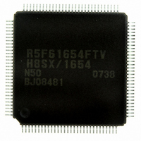
DF61654N50FTV Renesas Electronics America, DF61654N50FTV Datasheet - Page 33

DF61654N50FTV
Manufacturer Part Number
DF61654N50FTV
Description
IC H8SX/1654 MCU FLASH 120TQFP
Manufacturer
Renesas Electronics America
Series
H8® H8SX/1600r
Datasheet
1.DF61653N50FTV.pdf
(1020 pages)
Specifications of DF61654N50FTV
Core Processor
H8SX
Core Size
32-Bit
Speed
50MHz
Connectivity
I²C, IrDA, SCI, SmartCard, USB
Peripherals
DMA, PWM, WDT
Number Of I /o
75
Program Memory Size
512KB (512K x 8)
Program Memory Type
FLASH
Ram Size
40K x 8
Voltage - Supply (vcc/vdd)
3 V ~ 3.6 V
Data Converters
A/D 8x10b; D/A 2x8b
Oscillator Type
External
Operating Temperature
-20°C ~ 75°C
Package / Case
120-TQFP, 120-VQFP
For Use With
HS0005KCU11H - EMULATOR E10A-USB H8S(X),SH2(A)3DK1657 - DEV EVAL KIT FOR H8SX/1657
Lead Free Status / RoHS Status
Lead free / RoHS Compliant
Eeprom Size
-
Available stocks
Company
Part Number
Manufacturer
Quantity
Price
Company:
Part Number:
DF61654N50FTV
Manufacturer:
Renesas Electronics America
Quantity:
10 000
- Current page: 33 of 1020
- Download datasheet (6Mb)
Figure 8.9 Memory Map in Block Transfer Mode
Figure 8.10 Operation of Chain Transfer.................................................................................... 330
Figure 8.11 DTC Operation Timing (Example of Short Address Mode
Figure 8.12 DTC Operation Timing (Example of Short Address Mode
Figure 8.13 DTC Operation Timing (Example of Short Address Mode in Chain Transfer) ...... 332
Figure 8.14 DTC Operation Timing (Example of Full Address Mode
Figure 8.15 DTC with Interrupt Activation ................................................................................ 335
Figure 8.16 Chain Transfer when Counter = 0 ........................................................................... 338
Section 10 16-Bit Timer Pulse Unit (TPU)
Figure 10.1 Block Diagram of TPU............................................................................................ 398
Figure 10.2 Example of Counter Operation Setting Procedure .................................................. 435
Figure 10.3 Free-Running Counter Operation ............................................................................ 436
Figure 10.4 Periodic Counter Operation..................................................................................... 437
Figure 10.5 Example of Setting Procedure for Waveform Output by Compare Match.............. 437
Figure 10.6 Example of 0-Output/1-Output Operation............................................................... 438
Figure 10.7 Example of Toggle Output Operation ..................................................................... 438
Figure 10.8 Example of Setting Procedure for Input Capture Operation.................................... 439
Figure 10.9 Example of Input Capture Operation....................................................................... 440
Figure 10.10 Example of Synchronous Operation Setting Procedure ........................................ 441
Figure 10.11 Example of Synchronous Operation...................................................................... 442
Figure 10.12 Compare Match Buffer Operation......................................................................... 443
Figure 10.13 Input Capture Buffer Operation............................................................................. 444
Figure 10.14 Example of Buffer Operation Setting Procedure................................................... 444
Figure 10.15 Example of Buffer Operation (1)........................................................................... 445
Figure 10.16 Example of Buffer Operation (2)........................................................................... 446
Figure 10.17 Example of Cascaded Operation Setting Procedure .............................................. 447
Figure 10.18 Example of Cascaded Operation (1)...................................................................... 448
Figure 10.19 Example of Cascaded Operation (2)...................................................................... 448
Figure 10.20 Example of PWM Mode Setting Procedure .......................................................... 451
Figure 10.21 Example of PWM Mode Operation (1) ................................................................. 451
Figure 10.22 Example of PWM Mode Operation (2) ................................................................. 452
Figure 10.23 Example of PWM Mode Operation (3) ................................................................. 453
Figure 10.24 Example of Phase Counting Mode Setting Procedure........................................... 454
Figure 10.25 Example of Phase Counting Mode 1 Operation .................................................... 455
Figure 10.26 Example of Phase Counting Mode 2 Operation .................................................... 456
Figure 10.27 Example of Phase Counting Mode 3 Operation .................................................... 457
(When Transfer Destination is Specified as Block Area) .......................................... 329
in Normal Transfer Mode or Repeat Transfer Mode) .............................................. 332
in Normal Transfer Mode or Repeat Transfer Mode) ............................................. 331
in Block Transfer Mode with Block Size of 2) ....................................................... 331
Rev.1.00 Sep. 08, 2005 Page xxxi of xlviii
Related parts for DF61654N50FTV
Image
Part Number
Description
Manufacturer
Datasheet
Request
R

Part Number:
Description:
KIT STARTER FOR M16C/29
Manufacturer:
Renesas Electronics America
Datasheet:

Part Number:
Description:
KIT STARTER FOR R8C/2D
Manufacturer:
Renesas Electronics America
Datasheet:

Part Number:
Description:
R0K33062P STARTER KIT
Manufacturer:
Renesas Electronics America
Datasheet:

Part Number:
Description:
KIT STARTER FOR R8C/23 E8A
Manufacturer:
Renesas Electronics America
Datasheet:

Part Number:
Description:
KIT STARTER FOR R8C/25
Manufacturer:
Renesas Electronics America
Datasheet:

Part Number:
Description:
KIT STARTER H8S2456 SHARPE DSPLY
Manufacturer:
Renesas Electronics America
Datasheet:

Part Number:
Description:
KIT STARTER FOR R8C38C
Manufacturer:
Renesas Electronics America
Datasheet:

Part Number:
Description:
KIT STARTER FOR R8C35C
Manufacturer:
Renesas Electronics America
Datasheet:

Part Number:
Description:
KIT STARTER FOR R8CL3AC+LCD APPS
Manufacturer:
Renesas Electronics America
Datasheet:

Part Number:
Description:
KIT STARTER FOR RX610
Manufacturer:
Renesas Electronics America
Datasheet:

Part Number:
Description:
KIT STARTER FOR R32C/118
Manufacturer:
Renesas Electronics America
Datasheet:

Part Number:
Description:
KIT DEV RSK-R8C/26-29
Manufacturer:
Renesas Electronics America
Datasheet:

Part Number:
Description:
KIT STARTER FOR SH7124
Manufacturer:
Renesas Electronics America
Datasheet:

Part Number:
Description:
KIT STARTER FOR H8SX/1622
Manufacturer:
Renesas Electronics America
Datasheet:

Part Number:
Description:
KIT DEV FOR SH7203
Manufacturer:
Renesas Electronics America
Datasheet:


