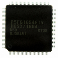
DF61654N50FTV Renesas Electronics America, DF61654N50FTV Datasheet - Page 638

DF61654N50FTV
Manufacturer Part Number
DF61654N50FTV
Description
IC H8SX/1654 MCU FLASH 120TQFP
Manufacturer
Renesas Electronics America
Series
H8® H8SX/1600r
Datasheet
1.DF61653N50FTV.pdf
(1020 pages)
Specifications of DF61654N50FTV
Core Processor
H8SX
Core Size
32-Bit
Speed
50MHz
Connectivity
I²C, IrDA, SCI, SmartCard, USB
Peripherals
DMA, PWM, WDT
Number Of I /o
75
Program Memory Size
512KB (512K x 8)
Program Memory Type
FLASH
Ram Size
40K x 8
Voltage - Supply (vcc/vdd)
3 V ~ 3.6 V
Data Converters
A/D 8x10b; D/A 2x8b
Oscillator Type
External
Operating Temperature
-20°C ~ 75°C
Package / Case
120-TQFP, 120-VQFP
For Use With
HS0005KCU11H - EMULATOR E10A-USB H8S(X),SH2(A)3DK1657 - DEV EVAL KIT FOR H8SX/1657
Lead Free Status / RoHS Status
Lead free / RoHS Compliant
Eeprom Size
-
Available stocks
Company
Part Number
Manufacturer
Quantity
Price
Company:
Part Number:
DF61654N50FTV
Manufacturer:
Renesas Electronics America
Quantity:
10 000
- Current page: 638 of 1020
- Download datasheet (6Mb)
Section 14 Serial Communication Interface (SCI, IrDA, CRC)
14.4.2
In asynchronous mode, the SCI operates on a base clock with a frequency of 16 times* the bit rate.
In reception, the SCI samples the falling edge of the start bit using the base clock, and performs
internal synchronization. Since receive data is sampled at the rising edge of the 8th pulse* of the
base clock, data is latched at the middle of each bit, as shown in figure 14.6. Thus the reception
margin in asynchronous mode is determined by formula (1) below.
Assuming values of F = 0 and D = 0.5 in formula (1), the reception margin is determined by the
formula below.
However, this is only the computed value, and a margin of 20% to 30% should be allowed in
system design.
Note: * This is an example when the ABCS bit in SEMR_2, 5, and 6 is 0. When the ABCS bit
Rev.1.00 Sep. 08, 2005 Page 588 of 966
REJ09B0219-0100
Internal basic
clock
Receive data
(RxD)
Synchronization
sampling timing
Data sampling
timing
[Legend]
M = ( 0.5 –
M: Reception margin
N: Ratio of bit rate to clock (When ABCS = 0, N = 16. When ABCS = 1, N = 8.)
D: Duty cycle of clock (D = 0.5 to 1.0)
L: Frame length (L = 9 to 12)
F: Absolute value of clock frequency deviation
M = | (0.5 –
Receive Data Sampling Timing and Reception Margin in Asynchronous Mode
is 1, a frequency of 8 times the bit rate is used as a base clock and receive data is
sampled at the rising edge of the 4th pulse of the base clock.
Figure 14.6 Receive Data Sampling Timing in Asynchronous Mode
2 × 16
2N
1
1
0
) – (L – 0.5) F –
) × 100
8 clocks
Start bit
[%] = 46.875%
16 clocks
7
| D – 0.5 |
N
(1
F ) | × 100
15 0
D0
[%]
... Formula (1)
7
15 0
D1
Related parts for DF61654N50FTV
Image
Part Number
Description
Manufacturer
Datasheet
Request
R

Part Number:
Description:
KIT STARTER FOR M16C/29
Manufacturer:
Renesas Electronics America
Datasheet:

Part Number:
Description:
KIT STARTER FOR R8C/2D
Manufacturer:
Renesas Electronics America
Datasheet:

Part Number:
Description:
R0K33062P STARTER KIT
Manufacturer:
Renesas Electronics America
Datasheet:

Part Number:
Description:
KIT STARTER FOR R8C/23 E8A
Manufacturer:
Renesas Electronics America
Datasheet:

Part Number:
Description:
KIT STARTER FOR R8C/25
Manufacturer:
Renesas Electronics America
Datasheet:

Part Number:
Description:
KIT STARTER H8S2456 SHARPE DSPLY
Manufacturer:
Renesas Electronics America
Datasheet:

Part Number:
Description:
KIT STARTER FOR R8C38C
Manufacturer:
Renesas Electronics America
Datasheet:

Part Number:
Description:
KIT STARTER FOR R8C35C
Manufacturer:
Renesas Electronics America
Datasheet:

Part Number:
Description:
KIT STARTER FOR R8CL3AC+LCD APPS
Manufacturer:
Renesas Electronics America
Datasheet:

Part Number:
Description:
KIT STARTER FOR RX610
Manufacturer:
Renesas Electronics America
Datasheet:

Part Number:
Description:
KIT STARTER FOR R32C/118
Manufacturer:
Renesas Electronics America
Datasheet:

Part Number:
Description:
KIT DEV RSK-R8C/26-29
Manufacturer:
Renesas Electronics America
Datasheet:

Part Number:
Description:
KIT STARTER FOR SH7124
Manufacturer:
Renesas Electronics America
Datasheet:

Part Number:
Description:
KIT STARTER FOR H8SX/1622
Manufacturer:
Renesas Electronics America
Datasheet:

Part Number:
Description:
KIT DEV FOR SH7203
Manufacturer:
Renesas Electronics America
Datasheet:


