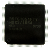
DF61654N50FTV Renesas Electronics America, DF61654N50FTV Datasheet - Page 241

DF61654N50FTV
Manufacturer Part Number
DF61654N50FTV
Description
IC H8SX/1654 MCU FLASH 120TQFP
Manufacturer
Renesas Electronics America
Series
H8® H8SX/1600r
Datasheet
1.DF61653N50FTV.pdf
(1020 pages)
Specifications of DF61654N50FTV
Core Processor
H8SX
Core Size
32-Bit
Speed
50MHz
Connectivity
I²C, IrDA, SCI, SmartCard, USB
Peripherals
DMA, PWM, WDT
Number Of I /o
75
Program Memory Size
512KB (512K x 8)
Program Memory Type
FLASH
Ram Size
40K x 8
Voltage - Supply (vcc/vdd)
3 V ~ 3.6 V
Data Converters
A/D 8x10b; D/A 2x8b
Oscillator Type
External
Operating Temperature
-20°C ~ 75°C
Package / Case
120-TQFP, 120-VQFP
For Use With
HS0005KCU11H - EMULATOR E10A-USB H8S(X),SH2(A)3DK1657 - DEV EVAL KIT FOR H8SX/1657
Lead Free Status / RoHS Status
Lead free / RoHS Compliant
Eeprom Size
-
Available stocks
Company
Part Number
Manufacturer
Quantity
Price
Company:
Part Number:
DF61654N50FTV
Manufacturer:
Renesas Electronics America
Quantity:
10 000
- Current page: 241 of 1020
- Download datasheet (6Mb)
6.7.6
When the byte control SRAM space is specified, the RDNCR setting for the corresponding space
is invalid.
The read strobe negation timing is the same timing as when RDNn = 1 in the basic bus interface.
Note that the RD timing with respect to the DACK rising edge becomes different.
6.7.7
In the byte control SRAM interface, the extension cycles can be inserted before and after the bus
cycle in the same way as the basic bus interface. For details, refer to section 6.6.6, Extension of
Chip Select (CS) Assertion Period.
6.7.8
For DMAC single address transfers, the DACK signal assert timing can be modified by using the
DKC bit in BCR1.
Figure 6.27 shows the DACK signal output timing. Setting the DKC bit to 1 asserts the DACK
signal a half cycle earlier.
Read Strobe (RD)
Extension of Chip Select (CS) Assertion Period
DACK Signal Output Timing
Rev.1.00 Sep. 08, 2005 Page 191 of 966
Section 6 Bus Controller (BSC)
REJ09B0219-0100
Related parts for DF61654N50FTV
Image
Part Number
Description
Manufacturer
Datasheet
Request
R

Part Number:
Description:
KIT STARTER FOR M16C/29
Manufacturer:
Renesas Electronics America
Datasheet:

Part Number:
Description:
KIT STARTER FOR R8C/2D
Manufacturer:
Renesas Electronics America
Datasheet:

Part Number:
Description:
R0K33062P STARTER KIT
Manufacturer:
Renesas Electronics America
Datasheet:

Part Number:
Description:
KIT STARTER FOR R8C/23 E8A
Manufacturer:
Renesas Electronics America
Datasheet:

Part Number:
Description:
KIT STARTER FOR R8C/25
Manufacturer:
Renesas Electronics America
Datasheet:

Part Number:
Description:
KIT STARTER H8S2456 SHARPE DSPLY
Manufacturer:
Renesas Electronics America
Datasheet:

Part Number:
Description:
KIT STARTER FOR R8C38C
Manufacturer:
Renesas Electronics America
Datasheet:

Part Number:
Description:
KIT STARTER FOR R8C35C
Manufacturer:
Renesas Electronics America
Datasheet:

Part Number:
Description:
KIT STARTER FOR R8CL3AC+LCD APPS
Manufacturer:
Renesas Electronics America
Datasheet:

Part Number:
Description:
KIT STARTER FOR RX610
Manufacturer:
Renesas Electronics America
Datasheet:

Part Number:
Description:
KIT STARTER FOR R32C/118
Manufacturer:
Renesas Electronics America
Datasheet:

Part Number:
Description:
KIT DEV RSK-R8C/26-29
Manufacturer:
Renesas Electronics America
Datasheet:

Part Number:
Description:
KIT STARTER FOR SH7124
Manufacturer:
Renesas Electronics America
Datasheet:

Part Number:
Description:
KIT STARTER FOR H8SX/1622
Manufacturer:
Renesas Electronics America
Datasheet:

Part Number:
Description:
KIT DEV FOR SH7203
Manufacturer:
Renesas Electronics America
Datasheet:


